
 German
 Japanese
 Portuguese
 Korea
Korea
 Mexico
 Dutch
Dutch


onsemi
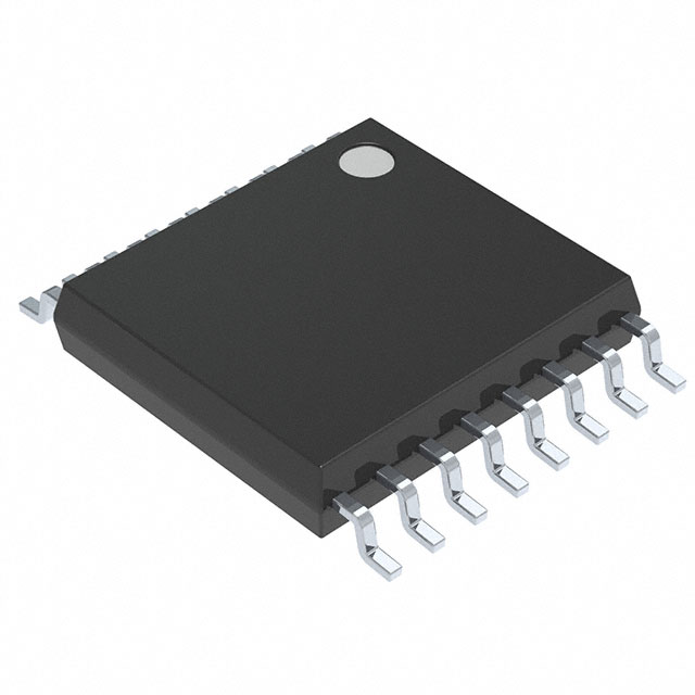
NB3V1108CDTR2G

Why Choose Us?
Professional Platform
B2B & B2C purchasingDelivery at full speed
1-2 days deliveryWide variety
Original manufacturers365 days guarantee
Responsible quality
.png)


Tech Specifications
NB3V1108CDTR2G Description
NB3V1108CDTR2G Description
The NB3V1108CDTR2G is a high-performance clock buffer IC designed for efficient signal distribution in a wide range of electronic systems. Manufactured by onsemi, this device is part of the Clock/Timing ICs category and is specifically engineered to provide reliable and precise clock signal distribution. The NB3V1108CDTR2G features an input-to-output ratio of 1:8, enabling it to distribute a single input clock signal to eight output lines. This fanout buffer operates within a supply voltage range of 1.71V to 3.6V, making it versatile for various power supply configurations. The device supports LVCMOS input and output levels, ensuring compatibility with a broad range of digital circuits. With a maximum operating frequency of 250 MHz, the NB3V1108CDTR2G is well-suited for high-speed applications requiring precise timing and minimal signal degradation.
NB3V1108CDTR2G Features
- High Fanout Capability: The 1:8 input-to-output ratio allows for efficient distribution of clock signals across multiple circuits, reducing the need for multiple buffer stages.
- Wide Supply Voltage Range: The device operates within a supply voltage range of 1.71V to 3.6V, providing flexibility in power supply design and compatibility with various system architectures.
- LVCMOS Compatibility: Both input and output levels are compatible with LVCMOS standards, ensuring seamless integration with modern digital systems.
- High-Speed Performance: With a maximum operating frequency of 250 MHz, the NB3V1108CDTR2G is ideal for high-speed applications requiring precise timing and minimal signal distortion.
- Surface Mount Technology: The surface mount package type facilitates easy integration into compact and high-density PCB designs.
- Compliance and Reliability: The NB3V1108CDTR2G is REACH unaffected and RoHS3 compliant, ensuring environmental safety and regulatory compliance. Additionally, it has a moisture sensitivity level (MSL) of 1, indicating unlimited storage life under standard conditions.
- Packaging: Available in a Tape & Reel (TR) package, the NB3V1180CDTR2G is suitable for automated assembly processes, enhancing manufacturing efficiency.
NB3V1108CDTR2G Applications
- Telecommunications: Ideal for distributing clock signals in high-speed communication systems, ensuring synchronized data transmission and reception.
- Networking: Used in network interface cards and routers to provide reliable clock distribution for multiple ports.
- Consumer Electronics: Suitable for applications such as high-definition televisions and gaming consoles, where precise timing is crucial for video and audio processing.
- Industrial Automation: Provides accurate clock distribution in PLCs and other industrial control systems, ensuring reliable operation of critical processes.
- Medical Equipment: Ensures precise timing in medical imaging and diagnostic devices, contributing to accurate and reliable performance.
Conclusion of NB3V1108CDTR2G
The NB3V1108CDTR2G is a robust and versatile clock buffer IC that offers significant advantages in high-speed signal distribution. Its wide supply voltage range, LVCMOS compatibility, and high operating frequency make it an ideal choice for a variety of applications, from telecommunications to consumer electronics. The device's compliance with environmental and regulatory standards, along with its surface mount package and unlimited moisture sensitivity level, ensures ease of integration and long-term reliability. Whether used in networking equipment, medical devices, or industrial control systems, the NB3V1108CDTR2G provides a reliable and efficient solution for clock signal distribution, making it a standout choice in the electronics industry.
FAQ
| Quantity | Unit Price | Ext. Price |
|---|---|---|
| 1+ | $4.78720 | $4.79 |
| 10+ | $3.13544 | $31.35 |
| 25+ | $2.70406 | $67.60 |
| 100+ | $2.21619 | $221.62 |
| 250+ | $1.97662 | $494.16 |
Not available to buy online? Want the lower wholesale price? Please Send RFQ to get best price, we will respond immediately


.png?x-oss-process=image/format,webp/resize,h_32)


