
 German
 Japanese
 Portuguese
 Korea
Korea
 Mexico
 Dutch
Dutch


onsemi
NB6L11SMNG

Why Choose Us?
Professional Platform
B2B & B2C purchasingDelivery at full speed
1-2 days deliveryWide variety
Original manufacturers365 days guarantee
Responsible quality
.png)


Tech Specifications
NB6L11SMNG Description
NB6L11SMNG Description
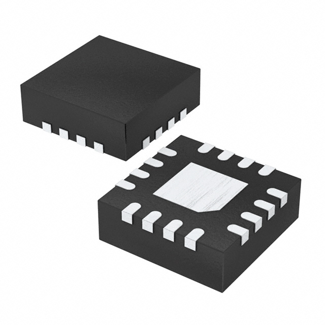
The NB6L11SMNG from onsemi is a high-performance 1:2 fanout buffer/translator designed for precision clock distribution and signal translation in demanding electronic systems. Part of the AnyLevel™ series, this surface-mount IC supports a wide range of input standards (CML, LVCMOS, LVDS, LVPECL, LVTTL) and delivers LVDS outputs, ensuring compatibility with diverse system requirements. Operating within a 2.375V to 2.625V supply range, it achieves exceptional signal integrity at frequencies up to 2 GHz, making it ideal for high-speed applications. The device is ROHS3 compliant, REACH unaffected, and housed in a 16-QFN package, suitable for automated assembly.
NB6L11SMNG Features
- High-Speed Performance: Supports frequencies up to 2 GHz with low jitter, critical for timing-sensitive applications.
- Versatile Input Compatibility: Accepts CML, LVCMOS, LVDS, LVPECL, and LVTTL inputs, enabling seamless integration into multi-standard designs.
- Differential Signaling: Features differential inputs and outputs (LVDS) for noise immunity and signal integrity.
- Low Power Operation: Optimized for 2.5V supply, reducing power consumption in high-frequency systems.
- Robust Packaging: 16-QFN surface-mount package with MSL1 (Unlimited) rating, ensuring reliability in manufacturing.
- Industry Compliance: ROHS3, REACH, and EAR99 certifications, meeting global environmental and export standards.
NB6L11SMNG Applications
- Telecommunications: Clock distribution in 5G base stations, optical transceivers, and network switches.
- Data Centers: High-speed signal buffering for servers, routers, and FPGAs.
- Test & Measurement: Precision timing for oscilloscopes, signal generators, and ATE systems.
- Industrial Electronics: Synchronization in automation controls and high-speed ADCs/DACs.
- Consumer Electronics: LVDS signal translation in high-resolution displays and video interfaces.
Conclusion of NB6L11SMNG
The NB6L11SMNG stands out as a flexible, high-performance solution for clock distribution and level translation, combining broad input compatibility, LVDS outputs, and 2 GHz operation in a compact package. Its low jitter, differential signaling, and industry certifications make it a preferred choice for telecom, data center, and industrial applications where signal integrity and reliability are paramount. For engineers seeking a robust, multi-standard buffer, the NB6L11SMNG delivers exceptional value and performance.
FAQ
| Quantity | Unit Price | Ext. Price |
|---|---|---|
| 1+ | $13.46743 | $13.47 |
| 10+ | $11.64515 | $116.45 |
| 30+ | $10.53428 | $316.03 |
Not available to buy online? Want the lower wholesale price? Please Send RFQ to get best price, we will respond immediately


.png?x-oss-process=image/format,webp/resize,h_32)


