
 German
 Japanese
 Portuguese
 Korea
Korea
 Mexico
 Dutch
Dutch


onsemi
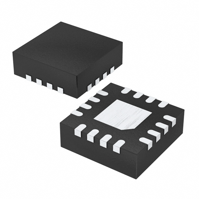
NB6L11SMNR2G

Why Choose Us?
Professional Platform
B2B & B2C purchasingDelivery at full speed
1-2 days deliveryWide variety
Original manufacturers365 days guarantee
Responsible quality
.png)


Tech Specifications
NB6L11SMNR2G Description
NB6L11SMNR2G Description
The NB6L11SMNR2G is a high-performance, AnyLevel™ series fanout buffer (distribution) and translator IC designed and manufactured by onsemi. This clock buffer is engineered to provide exceptional signal integrity and low jitter performance, making it ideal for a wide range of applications in the electronics industry. With a 1:2 input-to-output ratio, differential input and output, and a maximum frequency of 2 GHz, the NB6L11SMNR2G delivers outstanding performance in high-speed data transmission and clock distribution applications.
NB6L11SMNR2G Features
- ECCN: EAR99
- Ratio - Input:Output: 1:2
- Differential - Input:Output: Yes/Yes
- Mounting Type: Surface Mount
- Product Status: Active
- Series: AnyLevel™
- Type: Fanout Buffer (Distribution), Translator
- Input: CML, LVCMOS, LVDS, LVPECL, LVTTL
- Voltage - Supply: 2.375V ~ 2.625V
- Output: LVDS
- REACH Status: REACH Unaffected
- Manufacturer: onsemi
- HTSUS: 8542.39.0001
- Package: Tape & Reel (TR)
- Number of Circuits: 1
- Frequency - Max: 2 GHz
- RoHS Status: ROHS3 Compliant
- Base Product Number: NB6L11
- Moisture Sensitivity Level (MSL): 1 (Unlimited)
NB6L11SMNR2G Applications
The NB6L11SMNR2G is an ideal choice for various high-speed data transmission and clock distribution applications, including:
-
High-Speed Data Links: The NB6L11SMNR2G's differential input and output, along with its 2 GHz maximum frequency, make it suitable for high-speed data links in communication systems and networking equipment.
-
Clock Distribution: The 1:2 input-to-output ratio and low jitter performance of the NB6L11SMNR2G make it an excellent choice for clock distribution in high-speed digital systems, such as microprocessors, memory interfaces, and FPGAs.
-
Signal Integrity: The AnyLevel™ series fanout buffer's ability to handle various input types (CML, LVCMOS, LVDS, LVPECL, LVTTL) and its low jitter performance ensure excellent signal integrity in high-speed data transmission applications.
-
Automotive Applications: The NB6L11SMNR2G's robust performance and low jitter make it suitable for automotive applications, such as infotainment systems, advanced driver assistance systems (ADAS), and sensor interfaces.
Conclusion of NB6L11SMNR2G
The NB6L11SMNR2G from onsemi is a versatile and high-performance clock buffer and translator IC that offers exceptional signal integrity, low jitter performance, and a wide range of input compatibility. Its 1:2 input-to-output ratio, differential input and output, and maximum frequency of 2 GHz make it an ideal choice for high-speed data transmission and clock distribution applications in various industries, including communication systems, networking equipment, digital systems, and automotive applications. With its unique features and advantages over similar models, the NB6L11SMNR2G is a reliable and efficient solution for demanding high-speed data transmission and clock distribution requirements.
FAQ
| Quantity | Unit Price | Ext. Price |
|---|---|---|
| 1+ | $9.82960 | $9.83 |
| 10+ | $7.69472 | $76.95 |
| 25+ | $7.16179 | $179.04 |
| 100+ | $6.57606 | $657.61 |
| 250+ | $6.29693 | $1574.23 |
Not available to buy online? Want the lower wholesale price? Please Send RFQ to get best price, we will respond immediately


.png?x-oss-process=image/format,webp/resize,h_32)


