
 German
 Japanese
 Portuguese
 Korea
Korea
 Mexico
 Dutch
Dutch


onsemi
NB6N11SMNR2G

Why Choose Us?
Professional Platform
B2B & B2C purchasingDelivery at full speed
1-2 days deliveryWide variety
Original manufacturers365 days guarantee
Responsible quality
.png)


Tech Specifications
NB6N11SMNR2G Description
NB6N11SMNR2G Description
The NB6N11SMNR2G is a high-performance clock buffer and translator IC from onsemi, designed to meet the demanding requirements of modern electronic systems. With its AnyLevel™ ECLinPS MAX™ series, this device offers a 1:2 fanout ratio, differential input and output, and a maximum frequency of 2 GHz. The NB6N11SMNR2G is surface mountable, making it suitable for a wide range of applications.
NB6N11SMNR2G Features
- ECCN: EAR99
- Ratio - Input:Output: 1:2
- Differential - Input:Output: Yes/Yes
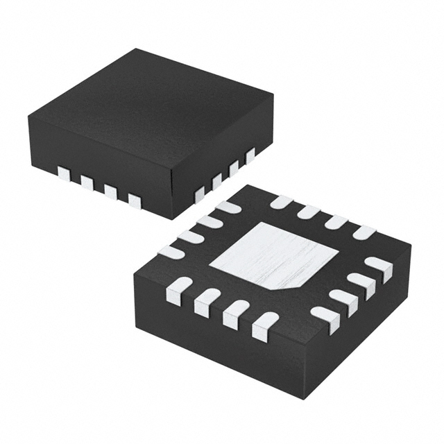
- Mounting Type: Surface Mount
- Product Status: Active
- Series: AnyLevel™ ECLinPS MAX™
- Type: Fanout Buffer (Distribution), Translator
- Input: CML, LVCMOS, LVDS, LVPECL, LVTTL
- Voltage - Supply: 3V ~ 3.6V
- Output: LVDS
- REACH Status: REACH Unaffected
- Mfr: onsemi
- HTSUS: 8542.39.0001
- Package: Tape & Reel (TR)
- Number of Circuits: 1
- Frequency - Max: 2 GHz
- RoHS Status: ROHS3 Compliant
- Base Product Number: NB6N11
- Moisture Sensitivity Level (MSL): 1 (Unlimited)
NB6N11SMNR2G Applications
The NB6N11SMNR2G is ideal for use in high-speed digital systems where clock distribution and translation are critical. Some specific use cases include:
- High-Speed Data Links: The device's 2 GHz maximum frequency makes it suitable for high-speed data links, such as those found in telecommunications and networking equipment.
- SerDes Applications: The NB6N11SMNR2G's LVDS output is ideal for Serializer/Deserializer (SerDes) applications, where high-speed data transmission is required.
- FPGA and ASIC Clock Distribution: The 1:2 fanout ratio and differential input/output make this IC suitable for clock distribution in FPGA and ASIC designs.
- Automotive Electronics: The NB6N11SMNR2G's robust performance and RoHS compliance make it suitable for use in automotive electronics, where high reliability and environmental resistance are essential.
Conclusion of NB6N11SMNR2G
The NB6N11SMNR2G is a versatile and high-performance clock buffer and translator IC from onsemi. Its unique features, such as differential input/output, 1:2 fanout ratio, and 2 GHz maximum frequency, make it an excellent choice for a wide range of high-speed digital systems. With its AnyLevel™ ECLinPS MAX™ series, the NB6N11SMNR2G offers superior performance and reliability, making it ideal for use in telecommunications, networking, SerDes applications, and automotive electronics.
FAQ
| Quantity | Unit Price | Ext. Price |
|---|---|---|
| 1+ | $11.07040 | $11.07 |
| 10+ | $7.62696 | $76.27 |
| 25+ | $6.72954 | $168.24 |
| 100+ | $5.71463 | $571.46 |
| 250+ | $5.48053 | $1370.13 |
Not available to buy online? Want the lower wholesale price? Please Send RFQ to get best price, we will respond immediately


.png?x-oss-process=image/format,webp/resize,h_32)


