
onsemi
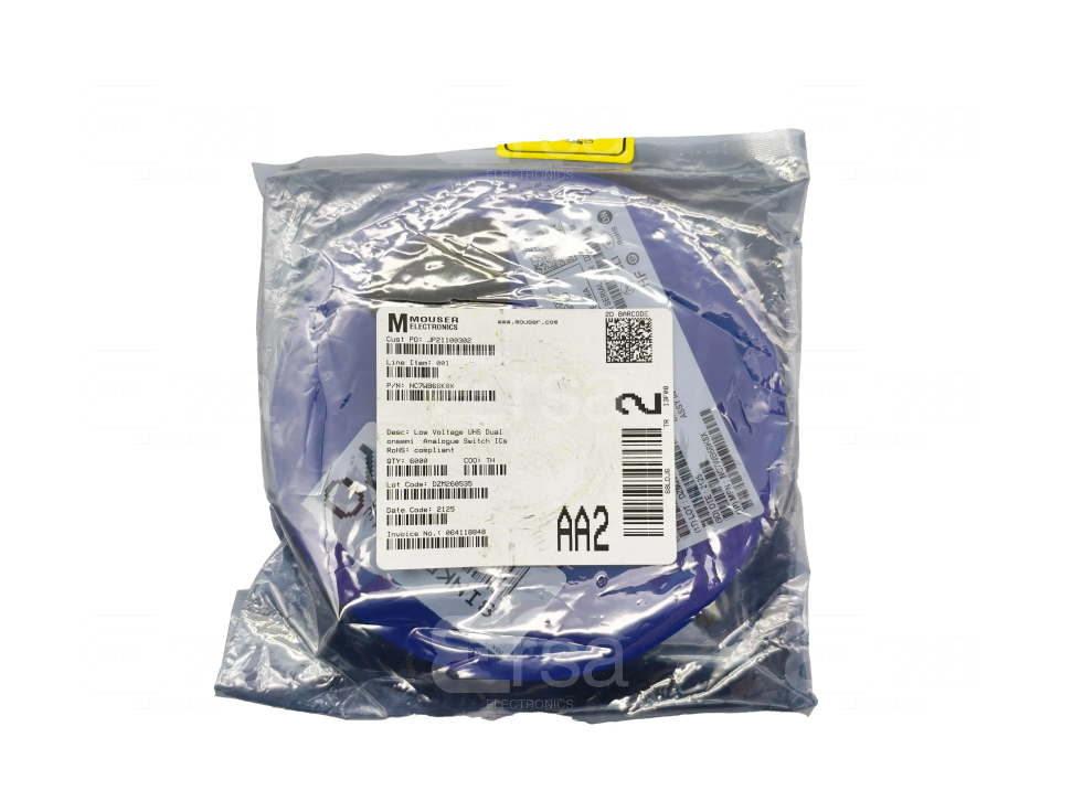
NC7WB66K8X
Analog Switches, Multiplexers, Demultiplexers


.png?x-oss-process=image/format,webp/resize,p_30)


NC7WB66K8X Description
NC7WB66K8X Description
The NC7WB66K8X is a surface-mount, single-pole single-throw normally open (SPST-NO) analog switch designed by onsemi. This device features two independent circuits, each offering a maximum on-state resistance (Ron) of 10Ω, ensuring minimal power loss and high efficiency in signal routing applications. The switch operates within a wide supply voltage range of 1.65V to 5.5V, making it suitable for various power supply configurations. The NC7WB66K8X is housed in a compact US8 package, which is ideal for space-constrained designs. Despite its small form factor, the device maintains excellent performance characteristics, including a leakage current (IS(off)) of only 100nA and a channel-to-channel matching (ΔRon) of 200mOhm. The switch also boasts a fast switching time of 3.2ns for turn-on and 4.1ns for turn-off, ensuring rapid signal transitions. The channel capacitance (CS(off), CD(off)) is kept low at 5pF, which helps in maintaining signal integrity at high frequencies. The device is REACH unaffected and RoHS3 compliant, adhering to stringent environmental regulations. The NC7WB66K8X is available in a tape and reel (TR) package, facilitating automated assembly processes.
NC7WB66K8X Features
- Low On-State Resistance: With a maximum on-state resistance of 10Ω, the NC7WB66K8X ensures minimal voltage drop and power dissipation, making it ideal for applications requiring high efficiency and low power loss.
- Wide Operating Voltage Range: The device operates within a supply voltage range of 1.65V to 5.5V, offering flexibility in various power supply configurations and ensuring compatibility with different system designs.
- Fast Switching Time: The NC7WB66K8X features a fast switching time of 3.2ns for turn-on and 4.1ns for turn-off, enabling rapid signal transitions and high-speed signal routing.
- Low Leakage Current: The maximum leakage current (IS(off)) is only 100nA, ensuring minimal power consumption in the off-state and maintaining low power dissipation.
- Channel-to-Channel Matching: The device offers a channel-to-channel matching (ΔRon) of 200mOhm, ensuring consistent performance across multiple channels and minimizing signal distortion.
- Low Channel Capacitance: The channel capacitance (CS(off), CD(off)) is kept low at 5pF, which helps in maintaining signal integrity at high frequencies and reducing signal degradation.
- Environmental Compliance: The NC7WB66K8X is REACH unaffected and RoHS3 compliant, adhering to stringent environmental regulations and ensuring suitability for a wide range of applications.
- Compact Packaging: Housed in a compact US8 package, the device is ideal for space-constrained designs and facilitates easy integration into various electronic systems.
- High Bandwidth: The device offers a -3dB bandwidth of 300MHz, making it suitable for high-frequency signal routing and ensuring minimal signal attenuation.
NC7WB66K8X Applications
The NC7WB66K8X is well-suited for a variety of applications where efficient signal routing and high performance are required. Some specific use cases include:
- Signal Routing in Communication Systems: The fast switching time and low on-state resistance make the NC7WB66K8X ideal for routing signals in communication systems, ensuring minimal signal degradation and high efficiency.
- Audio Signal Processing: The low channel capacitance and high bandwidth make the device suitable for audio signal processing applications, where maintaining signal integrity is crucial.
- Data Acquisition Systems: The device's low leakage current and wide operating voltage range make it ideal for data acquisition systems, ensuring accurate signal measurement and minimal power consumption.
- Medical Equipment: The compact packaging and environmental compliance make the NC7WB66K8X suitable for medical equipment, where space constraints and regulatory compliance are critical.
- Consumer Electronics: The device's high performance and low power consumption make it ideal for consumer electronics, ensuring efficient signal routing and minimal power loss.
Conclusion of NC7WB66K8X
The NC7WB66K8X is a high-performance analog switch designed for efficient signal routing and minimal power loss. Its low on-state resistance, fast switching time, and low leakage current make it suitable for a wide range of applications, including communication systems, audio signal processing, and data acquisition systems. The device's compact packaging and environmental compliance further enhance its suitability for various electronic designs. Despite its obsolete status, the NC7WB66K8X remains a reliable choice for applications requiring high efficiency and performance.
Tech Specifications
NC7WB66K8X Documents
Download datasheets and manufacturer documentation for NC7WB66K8X
Shopping Guide


.png?x-oss-process=image/format,webp/resize,h_32)


