
onsemi
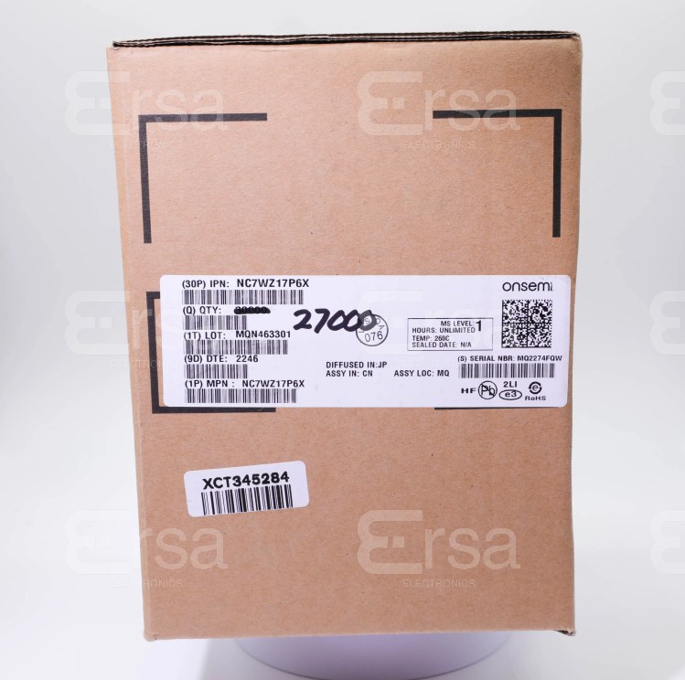
NC7WZ17P6X
Buffers, Drivers, Receivers, Transceivers


.png?x-oss-process=image/format,webp/resize,p_30)


NC7WZ17P6X Description
NC7WZ17P6X Description
The NC7WZ17P6X from onsemi is a high-performance, dual non-inverting buffer integrated circuit (IC) designed for low-voltage digital applications. Housed in a compact SC-88 (SOT-363) package, this Schmitt-trigger input device operates across a wide supply voltage range of 1.65V to 5.5V, making it versatile for mixed-voltage systems. With two independent 1-bit buffers, it ensures robust signal conditioning and noise immunity, ideal for interfacing between different logic levels. The device is RoHS3 compliant, REACH unaffected, and features a moisture sensitivity level (MSL) of 1, ensuring reliability in harsh environments. Its tape and reel (TR) packaging supports automated assembly processes, enhancing manufacturing efficiency.
NC7WZ17P6X Features
- Schmitt-Trigger Inputs: Provides hysteresis for improved noise rejection and signal integrity.
- Wide Voltage Range (1.65V–5.5V): Compatible with low-power and standard logic levels (e.g., 1.8V, 3.3V, 5V).
- High Drive Strength: 32mA output current (sink/source) enables direct driving of LEDs, relays, or other peripherals.
- Dual Non-Inverting Buffers: Independent channels for flexible signal routing.
- Space-Efficient SC-88 Package: Minimizes PCB footprint in portable and compact designs.
- Low Power Consumption: Optimized for battery-operated and energy-efficient applications.
- Robust Compliance: Meets ROHS3, REACH, and EAR99 standards for global deployment.
NC7WZ17P6X Applications
- Portable Electronics: Signal buffering in smartphones, tablets, and wearables due to low-voltage operation.
- Industrial Control Systems: Noise-immune interfacing for sensors, actuators, and PLCs.
- Automotive Electronics: Reliable level shifting in infotainment and ADAS modules.
- IoT Devices: Efficient signal conditioning for low-power wireless modules (BLE, Zigbee).
- Consumer Electronics: HDMI/USB signal integrity enhancement and GPIO expansion.
Conclusion of NC7WZ17P6X
The NC7WZ17P6X stands out for its Schmitt-trigger robustness, wide voltage flexibility, and high output drive, addressing critical challenges in modern digital designs. Its miniature form factor and compliance with environmental standards make it a preferred choice for space-constrained and eco-conscious applications. Whether for industrial automation, consumer gadgets, or automotive systems, this IC delivers reliable performance while simplifying design complexity. Engineers can leverage its noise immunity and low-power operation to enhance system reliability without compromising efficiency.
Tech Specifications
NC7WZ17P6X Documents
Download datasheets and manufacturer documentation for NC7WZ17P6X
 Assembly Change 10/Mar/2023
  NC7WZ17
  Mult Devices 24/Oct/2017 Binary Year Code Marking 15/Jan/2014
  Fab5 Supply Constraint 7/Mar/2022
  Available In the Digi-Key KiCad Library
  NC7SZ/NC7WZ/NC7NZ/NC7S/NC7ST 28/Dec/2020 Mult Dev DS Chgs 21/Sep/2020
  onsemi RoHS onsemi REACH
 Shopping Guide


.png?x-oss-process=image/format,webp/resize,h_32)


