onsemi_NCD5701CDR2G

onsemi
NCD5701CDR2G  
Gate Drivers ICs

onsemi
NCD5701CDR2G
730-NCD5701CDR2G
Ersa
onsemi-NCD5701CDR2G-datasheets-11561378.pdf
IC GATE DRVR HI/LOW SIDE 8SOIC
In Stock : 2097

Not available to buy online? Want the lower wholesale price? Please Send RFQ to get best price, we will respond immediately

QUICK RFQ
ADD TO RFQ LIST
ersa FreeSample ersa flow
ISO9001
Quality Policy
ISO45001
ISO14001

NCD5701CDR2G Description
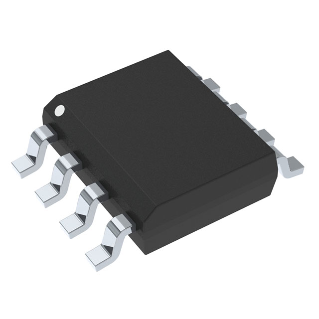
This electronic device regards Tape & Reel (TR) method as the top priority. This NCD5701CDR2G packaging method makes it simple and quick to package big quantities of powdered commodities. This NCD5701CDR2G is produced by this onsemi in order to provide enough products to meet consumers’ demand. The blueprint of this onsemi is to keep pace with the growth of world’s leading level of science and technology. This NCD5701CDR2G belongs to Gate Drivers ICs category. It’s previous category pertains to Power Management (PMIC). Complete power supply systems can be implemented using Power Management Integrated Circuits (PMICs). It combines several voltage regulators and control circuits onto a single chip. They simplify and cost-effectively manage system power management while reducing component count and board area. This NCD5701CDR2G is a great fit for embedded processing in a variety of applications. They are includes edge computing, the Internet of Things (IoT), industrial and medical IoT, electric vehicles (EVs), and autonomous cars.

Tech Specifications

Maximum Turn-On Delay Time (ns)
Latch-Up Proof
PPAP
Gate Type
Product Status
Automotive
Special Features
Supplier Package
Package / Case
Voltage - Supply
REACH Status
Channel Type
Maximum Operating Supply Voltage (V)
EU RoHS
Logic Voltage - VIL, VIH
Moisture Sensitivity Level (MSL)
Operating Temperature
Driven Configuration
Typical Input Low Threshold Voltage (V)
Maximum Fall Time (ns)
ECCN
Driver Type
Mounting Type
Standard Package Name
Current - Peak Output (Source, Sink)
Pin Count
Mounting
Driver Configuration
Lead Shape
HTSUS
Package
High and Low Sides Dependency
Rise / Fall Time (Typ)
Typical Input High Threshold Voltage (V)
PCB changed
HTS
ECCN (US)
Maximum Power Dissipation (mW)
Supplier Device Package
Minimum Operating Temperature (°C)
Maximum Operating Temperature (°C)
Peak Output Current (A)
Package Height
Mfr
RoHS Status
Input Type
Maximum Rise Time (ns)
Maximum Propagation Delay Time (ns)
Bridge Type
Number of Drivers
Package Length
Maximum Turn-Off Delay Time (ns)
Number of Outputs
Series
Type
Part Status
Reference Voltage (V)
Package Width
Base Product Number
Minimum Operating Supply Voltage (V)
Product
Fall Time
RoHS
Supply Voltage - Min
Operating Supply Current
Technology
Maximum Operating Temperature
Supply Voltage - Max
Mounting Style
Output Current
Minimum Operating Temperature
Rise Time
Maximum Turn-Off Delay Time
Shutdown
Maximum Turn-On Delay Time
Pd - Power Dissipation
USHTS
Output Voltage

NCD5701CDR2G Documents

Download datasheets and manufacturer documentation for NCD5701CDR2G

Ersa NCD570x 09/Mar/2023      
Ersa NCD5701A,B,C      
Ersa Mult MSL1 Pkg Rev 20/Dec/2018      
Ersa NCD5701A,B,C      
Ersa NCV5700/NCD5700/01 04/Apr/2018      
Ersa onsemi RoHS       Material Declaration NCD5701CDR2G       onsemi REACH      

Shopping Guide

Payment Methods
Payment Methods include Prepayment TT (bank transfer), Western Union, and PayPal. Customers are responsible for shipping costs, bank charges, customs duties and taxes.
Shipping Rate
Shipments are made once a day around 5pm, excluding Sundays. Once shipped, the estimated delivery time is usually 5-7 business days, depending on the courier you choose.
Delivery Methods
Provide DHL, FedEx, UPS, EMS, SF Express and Registered Airmail International Delivery Service