
 German
 Japanese
 Portuguese
 Korea
Korea
 Mexico
 Dutch
Dutch


Why Choose Us?
Professional Platform
B2B & B2C purchasingDelivery at full speed
1-2 days deliveryWide variety
Original manufacturers365 days guarantee
Responsible quality
.png)


Tech Specifications
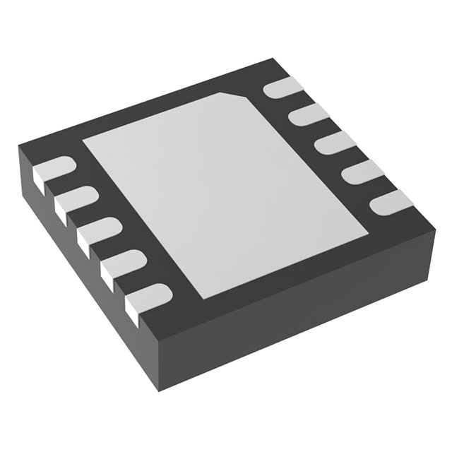
Package/Case
DFN
Halogen Free
Halogen Free
Lead Free
Lead Free
Max Input Voltage
3.6V
Min Input Voltage
1.1V
Max Operating Temperature
125°C
Min Operating Temperature
-40°C
Max Output Current
3A
NCP51510MNTWG Description
- LDO (Linear), DDR Voltage Regulator IC 1 Output 10-DFN (3x3)
FAQ
What voltage specification is listed for NCP51510MNTWG?
The listed voltage-related specification for NCP51510MNTWG is 3.6V.
What is the mounting type of NCP51510MNTWG?
Is NCP51510MNTWG currently in stock?
What operating temperature range does NCP51510MNTWG support?
What is NCP51510MNTWG?
Quick Quote
ADD TO RFQ LIST
Not available to buy online? Want the lower wholesale price? Please Send RFQ to get best price, we will respond immediately
QUICK RFQ


.png?x-oss-process=image/format,webp/resize,h_32)


