
onsemi
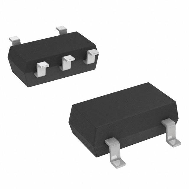
NCS333ASQ3T2G
OP Amps, Buffer Amps ICs


.png?x-oss-process=image/format,webp/resize,p_30)


NCS333ASQ3T2G Description
NCS333ASQ3T2G Description
The NCS333ASQ3T2G is a high-performance operational amplifier (op-amp) from onsemi, designed for precision applications requiring low noise, low drift, and high stability. With a supply voltage range of 1.8V to 5.5V, this op-amp is suitable for a wide range of power supply configurations. The device features a gain bandwidth product of 350 kHz and a -3dB bandwidth of 60 kHz, ensuring excellent frequency response for various applications. The slew rate of 0.15V/µs provides fast signal processing capabilities.
NCS333ASQ3T2G Features
- Low Input Bias Current: The NCS333ASQ3T2G boasts an ultra-low input bias current of 60 pA, which is crucial for maintaining signal integrity in high-impedance input applications.
- Zero-Drift Technology: This op-amp utilizes zero-drift technology, which minimizes the long-term drift in the output voltage, making it ideal for precision applications.
- Low Input Offset Voltage: With an input offset voltage of just 3.5 µV, the NCS333ASQ3T2G ensures high accuracy and stability in your circuit designs.
- Low Supply Current: The device consumes only 21 µA of supply current, making it suitable for battery-powered and power-sensitive applications.
- Surface Mount Packaging: The NCS333ASQ3T2G is available in a surface-mount package, which is ideal for space-constrained designs and automated assembly processes.
NCS333ASQ3T2G Applications
The NCS333ASQ3T2G is an excellent choice for a variety of applications where precision and stability are paramount. Some ideal use cases include:
- Sensor Signal Conditioning: The low drift and low noise characteristics make it suitable for conditioning signals from sensors in industrial and environmental monitoring applications.
- Precision Measurement Systems: The device's high stability and low offset voltage make it ideal for precision measurement systems, such as weigh scales and pressure transducers.
- Audio Applications: The NCS333ASQ3T2G can be used in audio preamplifiers and signal processing circuits where low noise and high fidelity are required.
- Medical Equipment: Due to its precision and stability, this op-amp is suitable for use in medical equipment, such as patient monitoring systems and diagnostic devices.
Conclusion of NCS333ASQ3T2G
The NCS333ASQ3T2G from onsemi is a versatile and high-performance operational amplifier that offers a unique combination of low noise, low drift, and high stability. Its wide supply voltage range, low input bias current, and zero-drift technology make it an ideal choice for precision applications in various industries. Whether you're designing sensor signal conditioning circuits, precision measurement systems, or audio equipment, the NCS333ASQ3T2G is a reliable and high-quality solution that delivers exceptional performance.
Tech Specifications
NCS333ASQ3T2G Documents
Download datasheets and manufacturer documentation for NCS333ASQ3T2G
 Wafer Fab and Assembly Change 21/Jul/2023
  NCS_NCV333(A)_2333_4333
  NCS_NCV333(A)_2333_4333
  onsemi RoHS Material Declaration NCS333ASQ3T2G
 Shopping Guide


.png?x-oss-process=image/format,webp/resize,h_32)


