
 German
 Japanese
 Portuguese
 Korea
Korea
 Mexico
 Dutch
Dutch


Why Choose Us?
Professional Platform
B2B & B2C purchasingDelivery at full speed
1-2 days deliveryWide variety
Original manufacturers365 days guarantee
Responsible quality
.png)


Tech Specifications
NE5517DR2 Description
NE5517DR2 Description
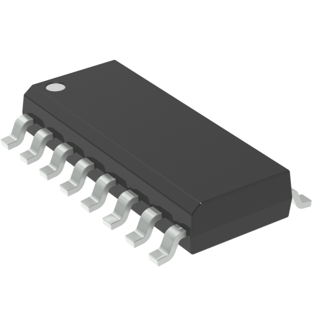
The NE5517DR2 is a high-performance transconductance operational amplifier designed by onsemi, a leading manufacturer in the electronics industry. This dual-channel IC is housed in a 16-pin SOIC package, making it suitable for surface-mount applications. Despite its obsolete status, the NE5517DR2 remains a robust choice for various analog signal processing tasks due to its wide voltage supply range, high slew rate, and low input bias current.
NE5517DR2 Features
- Wide Supply Voltage Range: The NE5517DR2 operates within a supply voltage span ranging from 4V to 44V, providing flexibility in power supply design and compatibility with a variety of power sources.
- High Slew Rate: With a slew rate of 50V/µs, this amplifier can handle high-frequency signals with minimal distortion, making it ideal for applications requiring fast transient response.
- Low Input Bias Current: The low input bias current of 400nA ensures high input impedance, which is crucial for minimizing loading effects on sensitive signal sources.
- High Gain Bandwidth Product: The 2MHz gain bandwidth product allows for high gain at relatively high frequencies, ensuring precise signal amplification across a broad spectrum.
- Low Input Offset Voltage: The input offset voltage of 400µV ensures accurate signal processing by minimizing inherent errors in the amplifier's operation.
- Dual-Channel Design: The NE5517DR2 features two independent circuits, allowing for simultaneous processing of two signals, which is beneficial in multi-channel systems.
- Surface Mount Technology (SMT): The surface-mount package type facilitates easy integration into modern PCB designs, enhancing reliability and reducing the overall footprint.
- Moisture Sensitivity Level (MSL) 1: This indicates that the device is not moisture-sensitive, making it suitable for a wide range of manufacturing environments without the need for special handling precautions.
NE5517DR2 Applications
The NE5517DR2 is well-suited for a variety of applications due to its versatile performance characteristics. Some specific use cases include:
- Audio Signal Processing: The high slew rate and low input bias current make it ideal for audio amplifiers, ensuring high-fidelity signal reproduction with minimal distortion.
- Analog Filters: The high gain bandwidth product and low offset input voltage are beneficial for designing precision analog filters, providing accurate and stable filtering across a wide frequency range.
- Sensor Signal Conditioning: The low input bias current and high input impedance are advantageous for interfacing with sensitive sensors, ensuring accurate and reliable signal conditioning.
- Communication Systems: The wide supply voltage range and high slew rate make it suitable for signal amplification in communication systems, where fast transient response and high reliability are critical.
Conclusion of NE5517DR2
The NE5517DR2, despite being marked as obsolete, continues to offer significant advantages in various electronic applications. Its wide supply voltage range, high slew rate, and low input bias current make it a reliable choice for high-performance analog signal processing. The dual-channel design and surface-mount package further enhance its versatility and ease of integration. While newer models may offer additional features, the NE5517DR2 remains a solid option for engineers seeking a proven and reliable transconductance amplifier.
FAQ
Not available to buy online? Want the lower wholesale price? Please Send RFQ to get best price, we will respond immediately


.png?x-oss-process=image/format,webp/resize,h_32)


