
 German
 Japanese
 Portuguese
 Korea
Korea
 Mexico
 Dutch
Dutch


onsemi
NL17SG08DFT2G

Why Choose Us?
Professional Platform
B2B & B2C purchasingDelivery at full speed
1-2 days deliveryWide variety
Original manufacturers365 days guarantee
Responsible quality
.png)


Tech Specifications
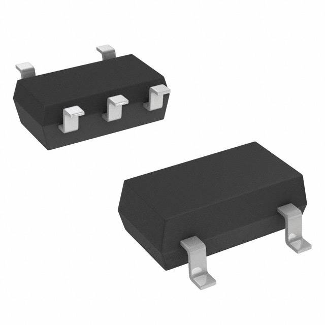
NL17SG08DFT2G Description
NL17SG08DFT2G Description
The NL17SG08DFT2G is a high-performance AND gate from onsemi, designed for use in a variety of electronic circuits. This device is part of the MiniGate™ series and offers excellent propagation delay and logic level performance. With a maximum propagation delay of 4.9ns at 3.3V and 30pF, it is ideal for high-speed applications. The NL17SG08DFT2G is a 2-input, 1-circuit AND gate, making it suitable for a wide range of digital logic functions.
NL17SG08DFT2G Features
- Logic Type: AND Gate
- Max Propagation Delay @ V, Max CL: 4.9ns @ 3.3V, 30pF
- Input Logic Level - Low: 0.7V ~ 0.8V
- Input Logic Level - High: 1.7V ~ 2V
- Voltage - Supply: 0.9V ~ 3.6V
- Current - Quiescent (Max): 500 nA
- Current - Output High, Low: 8mA, 8mA
- Mounting Type: Surface Mount
- Package: Tape & Reel (TR)
- RoHS Status: ROHS3 Compliant
- REACH Status: REACH Unaffected
- Moisture Sensitivity Level (MSL): 1 (Unlimited)
NL17SG08DFT2G Applications
The NL17SG08DFT2G is ideal for use in a variety of digital logic applications, including:
- Digital Signal Processing: Due to its low propagation delay and high-speed performance, it is suitable for use in digital signal processing circuits.
- Automotive Electronics: Its robust performance and compliance with RoHS and REACH regulations make it suitable for use in automotive electronics.
- Telecommunications: The NL17SG08DFT2G can be used in telecommunications equipment, where high-speed signal processing is required.
- Industrial Control Systems: Its ability to handle a wide range of supply voltages and input logic levels makes it suitable for use in industrial control systems.
Conclusion of NL17SG08DFT2G
The NL17SG08DFT2G is a high-performance AND gate from onsemi, offering excellent propagation delay and logic level performance. Its unique features, such as low quiescent current and wide supply voltage range, make it an ideal choice for a variety of digital logic applications. With its RoHS and REACH compliance, it is also suitable for use in environmentally conscious applications. Overall, the NL17SG08DFT2G is a reliable and high-performance solution for your digital logic needs.
FAQ
Not available to buy online? Want the lower wholesale price? Please Send RFQ to get best price, we will respond immediately


.png?x-oss-process=image/format,webp/resize,h_32)


