
 German
 Japanese
 Portuguese
 Korea
Korea
 Mexico
 Dutch
Dutch


onsemi
NL27WZ17DFT2G

Why Choose Us?
Professional Platform
B2B & B2C purchasingDelivery at full speed
1-2 days deliveryWide variety
Original manufacturers365 days guarantee
Responsible quality
.png)


Tech Specifications
NL27WZ17DFT2G Description
NL27WZ17DFT2G Description
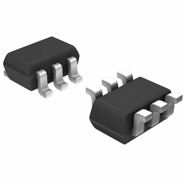
The NL27WZ17DFT2G from onsemi is a high-performance, dual non-inverting buffer with Schmitt-trigger inputs, designed for precision signal conditioning in low-voltage digital systems. Part of the 27WZ series, this logic IC operates across a wide supply voltage range of 1.65V to 5.5V, making it versatile for mixed-voltage applications. Housed in a compact SC88 package and delivered in Tape & Reel (TR), it is optimized for automated surface-mount assembly. The device complies with ROHS3 and REACH environmental standards, ensuring suitability for modern electronics manufacturing.
NL27WZ17DFT2G Features
- Schmitt-Trigger Inputs: Provides hysteresis for improved noise immunity and signal integrity in noisy environments.
- Wide Voltage Range (1.65V–5.5V): Supports compatibility with 1.8V, 3.3V, and 5V logic systems.
- High Output Drive (32mA sink/source): Capable of driving capacitive loads or multiple inputs with minimal propagation delay.
- Dual-Element Design: Integrates two independent buffers in a single package, saving board space.
- Low Power Consumption: Ideal for battery-powered and portable devices.
- MSL 1 (Unlimited): No moisture sensitivity concerns, simplifying storage and handling.
- Industrial-Grade Reliability: Meets EAR99 and HTSUS 8542.39.0001 classifications for global deployment.
NL27WZ17DFT2G Applications
This buffer is ideal for:
- Signal Conditioning: Cleaning up distorted or slow-rising signals in sensor interfaces or communication lines.
- Voltage Level Translation: Bridging between low-voltage microcontrollers and higher-voltage peripherals.
- Clock/Data Buffering: Ensuring robust signal distribution in FPGA, ASIC, or memory systems.
- Portable Electronics: Extending battery life in wearables, IoT devices, and handheld instruments.
- Automotive/Industrial Systems: Withstanding harsh environments due to its noise-resistant Schmitt-trigger design.
Conclusion of NL27WZ17DFT2G
The NL27WZ17DFT2G stands out for its low-voltage operation, high noise immunity, and compact footprint, making it a superior choice for space-constrained, noise-sensitive designs. Its dual-buffer configuration and ROHS3 compliance further enhance its appeal for eco-conscious and high-density PCB layouts. Whether for consumer electronics or industrial automation, this IC delivers reliable performance with minimal design overhead.
FAQ
| Quantity | Unit Price | Ext. Price |
|---|---|---|
| 100+ | $0.04829 | $4.83 |
| 300+ | $0.04193 | $12.58 |
| 3000+ | $0.03527 | $105.81 |
| 6000+ | $0.03144 | $188.64 |
| 9000+ | $0.02952 | $265.68 |
Not available to buy online? Want the lower wholesale price? Please Send RFQ to get best price, we will respond immediately


.png?x-oss-process=image/format,webp/resize,h_32)


