

onsemi
NLAS4599DFT2
Analog Switches, Multiplexers, Demultiplexers
Not available to buy online? Want the lower wholesale price? Please Send RFQ to get best price, we will respond immediately


.png?x-oss-process=image/format,webp/resize,p_30)


NLAS4599DFT2 Description
NLAS4599DFT2 Description
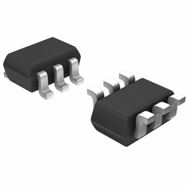
The NLAS4599DFT2 is a high-performance, single-pole double-throw (SPDT) switch designed by onsemi. This Interface IC Chip is optimized for a wide range of applications requiring reliable signal switching and minimal signal degradation. The NLAS4599DFT2 is housed in a Surface Mount package, specifically a SC88, and is available in Tape & Reel (TR) format, making it suitable for automated assembly processes.
NLAS4599DFT2 Features
- Low On-State Resistance: The NLAS4599DFT2 boasts a maximum on-state resistance (Ron) of 25Ω, ensuring minimal power loss and high efficiency during signal transmission.
- High Channel-to-Channel Matching: With a ΔRon of 2Ω, this IC ensures consistent performance across channels, making it ideal for applications requiring precise signal switching.
- Low Leakage Current: The maximum leakage current (IS(off)) is only 100nA, which helps in maintaining signal integrity and reducing power consumption.
- Fast Switching Times: The switch time (Ton, Toff) is 14ns and 8ns respectively, enabling rapid signal switching without significant delays.
- Wide Operating Voltage Range: The NLAS4599DFT2 operates within a supply voltage range of 2V to 5.5V, offering flexibility in various power supply configurations.
- Low Channel Capacitance: Both CS(off) and CD(off) are rated at 10pF, minimizing signal distortion and ensuring high-frequency performance.
- Wide Bandwidth: The -3dB bandwidth of 220MHz supports high-frequency applications, making it suitable for modern communication systems.
- Moisture Sensitivity Level (MSL) 1: The NLAS4599DFT2 is classified as MSL 1, indicating it is suitable for unlimited exposure to moisture, enhancing its reliability in various environmental conditions.
- Compliance: The NLAS4599DFT2 is REACH unaffected and classified under ECCN EAR99, ensuring compliance with international regulations.
NLAS4599DFT2 Applications
The NLAS4599DFT2 is designed for applications requiring high-speed signal switching and minimal signal degradation. Its low on-state resistance and fast switching times make it ideal for:
- Telecommunications: Switching high-frequency signals in communication systems.
- Data Acquisition Systems: Efficiently routing signals in data acquisition and control systems.
- Medical Equipment: Ensuring reliable signal transmission in medical devices.
- Automotive Electronics: Managing signal routing in automotive control systems.
- Consumer Electronics: Enhancing signal integrity in consumer devices such as smartphones and tablets.
Conclusion of NLAS4599DFT2
The NLAS4599DFT2 is a versatile and high-performance SPDT switch that offers significant advantages over similar models. Its low on-state resistance, high channel-to-channel matching, and fast switching times make it an excellent choice for applications requiring reliable and efficient signal switching. Despite being marked as obsolete, the NLAS4599DFT2 remains a robust solution for engineers and designers looking to optimize their signal routing needs.
Tech Specifications
NLAS4599DFT2 Documents
Download datasheets and manufacturer documentation for NLAS4599DFT2
Related Parts


Shopping Guide


.png?x-oss-process=image/format,webp/resize,h_32)


©2025 ERSA Electronics Corporation.