
 German
 Japanese
 Portuguese
 Korea
Korea
 Mexico
 Dutch
Dutch


onsemi
NLV14049UBDR2G
705-NLV14049UBDR2G

PDF Datasheet
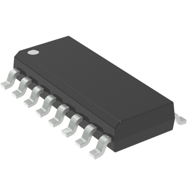
Hex Inverter, SOIC 16 LEAD, 2500-REEL
6 Weeks
Why Choose Us?
Professional Platform
B2B & B2C purchasingDelivery at full speed
1-2 days deliveryWide variety
Original manufacturers365 days guarantee
Responsible quality
.png)


Tech Specifications
Package/Case
SOIC
Halogen Free
Halogen Free
High Level Output Current
40mA
Lead Free
Lead Free
Logic Function
Inverter
Low Level Output Current
10mA
Max Operating Temperature
125°C
Min Operating Temperature
-55°C
NLV14049UBDR2G Description
Inverter IC 6 Channel 16-SOIC
FAQ
Does NLV14049UBDR2G have quantity-based pricing?
Yes. NLV14049UBDR2G currently has 13 pricing tier(s), starting from 1 units.
What is the standard lead time for NLV14049UBDR2G?
Are there related or alternative parts for NLV14049UBDR2G?
Is NLV14049UBDR2G currently in stock?
What is NLV14049UBDR2G?
Availability
(In Stock :
2069 )
| Quantity | Unit Price | Ext. Price |
|---|---|---|
| 1+ | $0.42240 | $0.42 |
| 10+ | $0.29392 | $2.94 |
| 25+ | $0.26224 | $6.56 |
| 100+ | $0.22766 | $22.77 |
| 250+ | $0.21116 | $52.79 |
Quick Quote
ADD TO RFQ LIST
Not available to buy online? Want the lower wholesale price? Please Send RFQ to get best price, we will respond immediately
QUICK RFQ


.png?x-oss-process=image/format,webp/resize,h_32)


