
onsemi
NLV74HC74ADTR2G
Flip Flops


.png?x-oss-process=image/format,webp/resize,p_30)


NLV74HC74ADTR2G Description
NLV74HC74ADTR2G Description
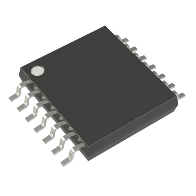
The NLV74HC74ADTR2G is a dual D-type flip-flop from onsemi, designed for high-speed digital applications. This Logic IC Chip features a clock frequency of up to 35 MHz, ensuring reliable performance in fast-paced digital circuits. It operates within a wide supply voltage range of 2V to 6V, making it versatile for various power supply configurations. The device supports complementary outputs, providing flexibility in circuit design and reducing the need for additional components.
NLV74HC74ADTR2G Features
- High-Speed Operation: With a maximum clock frequency of 35 MHz, the NLV74HC74ADTR2G is suitable for high-speed digital applications.
- Low Power Consumption: The device features a low quiescent current of 2 µA, making it energy-efficient and ideal for battery-powered or low-power systems.
- Wide Operating Voltage Range: The 2V to 6V supply voltage range allows for compatibility with a variety of power supply configurations.
- Complementary Outputs: The complementary output type provides flexibility in circuit design, reducing the need for additional inverters.
- Positive Edge Triggering: The flip-flop is triggered on the positive edge of the clock signal, ensuring precise timing control.
- Set and Reset Functionality: The device includes set (preset) and reset functions, providing additional control over the flip-flop's state.
- High Output Current Capability: The device can source and sink up to 5.2 mA, making it suitable for driving various loads.
- Low Input Capacitance: With an input capacitance of only 10 pF, the NLV74HC74ADTR2G minimizes loading effects on the driving circuit.
- Moisture Sensitivity Level 1: The device is classified as MSL 1 (Unlimited), making it suitable for extended storage and handling without special precautions.
- Compliance: The NLV74HC74ADTR2G is REACH unaffected and RoHS3 compliant, ensuring it meets environmental and regulatory standards.
NLV74HC74ADTR2G Applications
The NLV74HC74ADTR2G is ideal for a variety of applications due to its high-speed operation, low power consumption, and versatile features. Some specific use cases include:
- Digital Clock Circuits: The high clock frequency and precise edge triggering make it suitable for digital clock circuits where timing accuracy is critical.
- Data Latching and Storage: The dual D-type flip-flops can be used for data latching and storage in digital systems, ensuring data integrity and reliability.
- Synchronization Circuits: The device can be used in synchronization circuits to align data streams and ensure proper timing between different parts of a digital system.
- Sequential Logic Circuits: The set and reset functions make it suitable for sequential logic circuits where state control is essential.
- Low-Power Embedded Systems: The low quiescent current and wide operating voltage range make it ideal for low-power embedded systems, such as IoT devices and portable electronics.
Conclusion of NLV74HC74ADTR2G
The NLV74HC74ADTR2G from onsemi is a versatile and high-performance dual D-type flip-flop suitable for a wide range of digital applications. Its high-speed operation, low power consumption, and wide operating voltage range make it an excellent choice for modern digital circuits. The complementary outputs, positive edge triggering, and set/reset functionality provide additional design flexibility and control. While the product is now obsolete, its unique features and performance benefits make it a reliable option for existing designs and legacy systems.
Tech Specifications
NLV74HC74ADTR2G Documents
Download datasheets and manufacturer documentation for NLV74HC74ADTR2G
 NLV74 Series PCN Update 17 25/Jan/2024
  MC74HC74A
  DK OBS NOTICE
  MC74HC74A
  NLV74HC 9-29-22
  onsemi RoHS Material Declaration NLV74HC74ADTR2G
 Shopping Guide


.png?x-oss-process=image/format,webp/resize,h_32)


