
onsemi
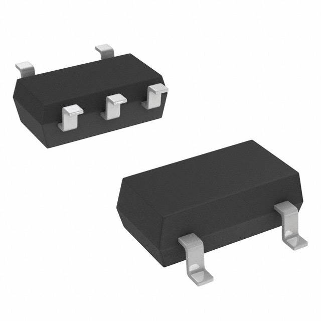
NS5B1G385DFT2G
Analog Switches, Multiplexers, Demultiplexers


.png?x-oss-process=image/format,webp/resize,p_30)


NS5B1G385DFT2G Description
NS5B1G385DFT2G Description
The NS5B1G385DFT2G is a high-performance analog switch manufactured by ON Semiconductor, designed for applications that require a low on-state resistance and fast switching times. With a maximum on-state resistance of 15 Ohms and a switch time of 6ns (Ton) and 2ns (Toff), this device is ideal for applications where signal integrity and speed are critical. The NS5B1G385DFT2G is a 1:1 multiplexer/demultiplexer circuit, providing a single channel with a capacitance of 4.1pF. It operates over a supply voltage range of 2V to 5.5V and has a -3dB bandwidth of 330MHz, making it suitable for high-frequency applications.
NS5B1G385DFT2G Features
- Low On-State Resistance: The NS5B1G385DFT2G offers a maximum on-state resistance of 15 Ohms, ensuring minimal signal loss and distortion.
- Fast Switching Times: With a maximum switch time of 6ns (Ton) and 2ns (Toff), this device is ideal for high-speed applications.
- Wide Supply Voltage Range: The NS5B1G385DFT2G operates over a supply voltage range of 2V to 5.5V, providing flexibility in power supply design.
- High Bandwidth: The -3dB bandwidth of 330MHz makes this device suitable for high-frequency applications.
- Low Channel Capacitance: The 4.1pF channel capacitance minimizes signal distortion and ensures fast signal propagation.
- Low Leakage Current: The maximum leakage current of 100nA helps to minimize power consumption in low-power applications.
NS5B1G385DFT2G Applications
The NS5B1G385DFT2G is ideal for a variety of applications where high performance, low on-state resistance, and fast switching times are required. Some specific use cases include:
- Audio and Video Processing: The low on-state resistance and high bandwidth make this device suitable for audio and video signal processing applications, ensuring minimal signal distortion and loss.
- Communications: The fast switching times and high bandwidth of the NS5B1G385DFT2G make it ideal for high-speed data communication applications, such as Ethernet and wireless communication systems.
- Automotive: This device can be used in automotive applications where high performance and reliability are critical, such as in-vehicle infotainment systems and sensor interfaces.
- Industrial Control: The NS5B1G385DFT2G can be used in industrial control systems where high-speed signal processing and low signal distortion are required.
Conclusion of NS5B1G385DFT2G
The NS5B1G385DFT2G is a high-performance analog switch that offers a combination of low on-state resistance, fast switching times, and high bandwidth, making it ideal for a variety of applications where signal integrity and speed are critical. Its unique features and advantages over similar models, such as low channel capacitance and low leakage current, further enhance its performance in demanding applications. While the product is now considered obsolete, it remains a reliable choice for applications that require a high-performance analog switch with fast switching capabilities.
Tech Specifications
NS5B1G385DFT2G Documents
Download datasheets and manufacturer documentation for NS5B1G385DFT2G
 NS5B1G385
  OBS NOTICE 11/Sep/2023
  NS5B1G385
  onsemi RoHS Material Declaration NS5B1G385DFT2G onsemi REACH
 Shopping Guide


.png?x-oss-process=image/format,webp/resize,h_32)


