
 German
 Japanese
 Portuguese
 Korea
Korea
 Mexico
 Dutch
Dutch


onsemi
NTMFD5C446NLT1G
289-NTMFD5C446NLT1G

PDF Datasheet
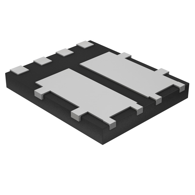
Dual N-Channel Power MOSFET 40 V, 145A, 2.65mΩ, 1500-REEL
19 Weeks
Why Choose Us?
Professional Platform
B2B & B2C purchasingDelivery at full speed
1-2 days deliveryWide variety
Original manufacturers365 days guarantee
Responsible quality
.png)


Tech Specifications
Max Operating Temperature
175
Number of Terminals
6
Min Operating Temperature
-55
Terminal Position
DUAL
Number of Elements
2
Lead Free
Yes
REACH
not_compliant
Military Spec
False
NTMFD5C446NLT1G Description
Mosfet Array 40V 25A (Ta), 145A (Tc) 3.5W (Ta), 125W (Tc) Surface Mount 8-DFN (5x6) Dual Flag (SO8FL-Dual)
FAQ
What is NTMFD5C446NLT1G?
NTMFD5C446NLT1G is a FET, MOSFET Arrays from onsemi. This product page provides its main specifications, pricing information, availability, and inquiry options.
What operating temperature range does NTMFD5C446NLT1G support?
Is NTMFD5C446NLT1G currently in stock?
What is the standard lead time for NTMFD5C446NLT1G?
Are there related or alternative parts for NTMFD5C446NLT1G?
Quick Quote
ADD TO RFQ LIST
Not available to buy online? Want the lower wholesale price? Please Send RFQ to get best price, we will respond immediately
QUICK RFQ


.png?x-oss-process=image/format,webp/resize,h_32)


