
 German
 Japanese
 Portuguese
 Korea
Korea
 Mexico
 Dutch
Dutch


onsemi
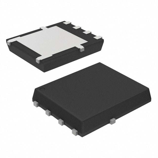
NTMFS006N12MCT1G

Why Choose Us?
Professional Platform
B2B & B2C purchasingDelivery at full speed
1-2 days deliveryWide variety
Original manufacturers365 days guarantee
Responsible quality
.png)


Tech Specifications
NTMFS006N12MCT1G Description
NTMFS006N12MCT1G Description
The NTMFS006N12MCT1G is a high-performance, single N-channel power MOSFET from onsemi. This MOSFET is designed for applications requiring high power dissipation and low on-resistance. With a drain-to-source voltage of 120V and a continuous drain current of up to 15A at 25°C, the NTMFS006N12MCT1G is ideal for use in a variety of power electronics applications.
NTMFS006N12MCT1G Features
- High Drain-to-Source Voltage (Vdss): 120V, making it suitable for high-voltage applications.
- Low On-Resistance (Rds On): 6mOhm at 46A and 10V, reducing power losses and improving efficiency.
- High Continuous Drain Current (Id): 15A at 25°C and 93A at Tc, providing high current handling capability.
- Low Gate Threshold Voltage (Vgs(th)): 4V at 260µA, enabling easy gate drive.
- Low Input Capacitance (Ciss): 3365 pF at 60V, reducing switching losses and improving efficiency.
- Low Gate Charge (Qg): 42 nC at 10V, reducing switching losses and improving efficiency.
- **Surface Mount Packaging:**PCB。
- Compliance with RoHS3 and REACH: Ensuring environmental compliance and reducing the risk of regulatory non-compliance.
NTMFS006N12MCT1G Applications
The NTMFS006N12MCT1G is ideal for a variety of power electronics applications, including:
- Power Supplies: Due to its high voltage and current ratings, it is suitable for use in power supply designs.
- Motor Controls: Its low on-resistance and high current capability make it suitable for motor control applications.
- Automotive Electronics: The high voltage rating and compliance with environmental regulations make it suitable for automotive electronics applications.
- Industrial Controls: Its robustness and high power dissipation capability make it suitable for use in industrial control systems.
Conclusion of NTMFS006N12MCT1G
The NTMFS006N12MCT1G from onsemi is a high-performance, single N-channel power MOSFET that offers a combination of high voltage, low on-resistance, and low gate charge. Its surface mount packaging and compliance with environmental regulations make it an ideal choice for a variety of power electronics applications. With its unique features and advantages, the NTMFS006N12MCT1G stands out from similar models and provides a reliable solution for high-power applications.
FAQ
Not available to buy online? Want the lower wholesale price? Please Send RFQ to get best price, we will respond immediately


.png?x-oss-process=image/format,webp/resize,h_32)


