
 German
 Japanese
 Portuguese
 Korea
Korea
 Mexico
 Dutch
Dutch


onsemi
NTMFS4934NT1G

Why Choose Us?
Professional Platform
B2B & B2C purchasingDelivery at full speed
1-2 days deliveryWide variety
Original manufacturers365 days guarantee
Responsible quality
.png)


Tech Specifications
NTMFS4934NT1G Description
NTMFS4934NT1G Description
The NTMFS4934NT1G is a high-performance N-Channel MOSFET from onsemi, designed for applications requiring robust power management and efficient switching. With a drain-to-source voltage (Vdss) of 30V and a continuous drain current (Id) of 17.1A at 25°C, this MOSFET is well-suited for a variety of power electronic applications.
NTMFS4934NT1G Features
- High Power Dissipation: Capable of handling up to 930mW at ambient temperature and 69.44W at case temperature, ensuring reliable operation in demanding conditions.
- Low On-Resistance: With a maximum Rds On of 2mOhm at 30A and 10V, the NTMFS4934NT1G minimizes power losses and improves efficiency.
- Robust Gate Drive: A gate charge (Qg) of 34 nC at 4.5V and a gate-source voltage (Vgs) range of ±20V provide stable and efficient gate control.
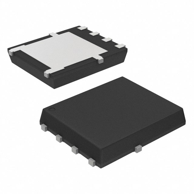
- Surface Mount Technology: The 5DFN package allows for compact and efficient PCB layout, ideal for space-constrained applications.
- Compliance and Sensitivity: ROHS3 compliant and moisture sensitivity level (MSL) 1, ensuring environmental and reliability standards are met.
NTMFS4934NT1G Applications
The NTMFS4934NT1G is ideal for applications where high power handling and efficient switching are critical, such as:
- Power Supplies: In switch-mode power supplies (SMPS) and battery chargers, where high efficiency and low power dissipation are required.
- Industrial Controls: For motor drives and inverter circuits, providing reliable switching and power management.
- Automotive Electronics: In electric vehicle (EV) charging systems and power management units, ensuring robust operation under various environmental conditions.
Conclusion of NTMFS4934NT1G
While the NTMFS4934NT1G is now considered obsolete, its legacy of high performance and reliability makes it a suitable choice for existing designs or where replacement parts are needed. Its unique combination of high power dissipation, low on-resistance, and robust gate drive capabilities make it an excellent choice for applications demanding high efficiency and reliability. Despite its obsolescence, the NTMFS4934NT1G remains a valuable component in the right application, offering a proven solution for power electronic challenges.
FAQ
Not available to buy online? Want the lower wholesale price? Please Send RFQ to get best price, we will respond immediately


.png?x-oss-process=image/format,webp/resize,h_32)


