onsemi_NTMFS4C55NT1G

onsemi
NTMFS4C55NT1G  
Single FETs, MOSFETs

onsemi
NTMFS4C55NT1G
278-NTMFS4C55NT1G
Ersa
onsemi-NTMFS4C55NT1G-datasheets-623804.pdf
MOSFET N-CH 30V 78A SO8FL
In Stock : 15961

Not available to buy online? Want the lower wholesale price? Please Send RFQ to get best price, we will respond immediately

QUICK RFQ
ADD TO RFQ LIST
ersa FreeSample ersa flow
ISO9001
Quality Policy
ISO45001
ISO14001

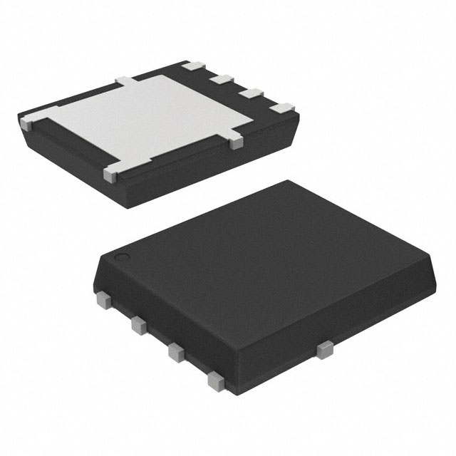
NTMFS4C55NT1G Description

The NTMFS4C55NT1G is a high voltage N-channel MOSFET transistor manufactured by ON Semiconductor. It is designed for use in a variety of applications, including high voltage switching and power management circuits.

Description:

The NTMFS4C55NT1G is an N-channel enhancement mode field effect transistor (MOSFET) with a drain-to-source voltage (VDS) of up to 500V. It has a continuous drain current (ID) of 4.5A and a gate-source voltage (VGS) of 10V. The device is available in a TO-220 package.

Features:

  • High voltage N-channel MOSFET
  • Drain-to-source voltage (VDS) of up to 500V
  • Continuous drain current (ID) of 4.5A
  • Gate-source voltage (VGS) of 10V
  • Low on-state resistance (RDS(on))
  • Suitable for use in high voltage switching and power management circuits

Applications:

  • High voltage switching applications
  • Power management circuits
  • Motor control applications
  • DC-DC converters
  • Class D audio amplifiers
  • Industrial control systems

The NTMFS4C55NT1G is a reliable and efficient MOSFET transistor that can be used in a variety of high voltage applications. Its high drain-to-source voltage and continuous drain current make it suitable for use in power management circuits and motor control applications. Its low on-state resistance also makes it an ideal choice for use in high efficiency switching applications.

Tech Specifications

Configuration
Typical Turn-Off Delay Time (ns)
Maximum Gate Source Leakage Current (nA)
Input Capacitance (Ciss) (Max) @ Vds
Gate Charge (Qg) (Max) @ Vgs
Typical Rise Time (ns)
PPAP
Channel Mode
Typical Turn-On Delay Time (ns)
Product Status
Automotive
Drain to Source Voltage (Vdss)
Supplier Package
Maximum IDSS (uA)
Package / Case
Technology
REACH Status
Channel Type
EU RoHS
Maximum Continuous Drain Current (A)
Moisture Sensitivity Level (MSL)
Operating Temperature
Maximum Drain Source Voltage (V)
Maximum Drain Source Resistance (mOhm)
ECCN
Mounting Type
Rds On (Max) @ Id, Vgs
Standard Package Name
Vgs(th) (Max) @ Id
Pin Count
Mounting
Lead Shape
Current - Continuous Drain (Id) @ 25°C
SVHC
Drive Voltage (Max Rds On, Min Rds On)
HTSUS
Package
Typical Gate Charge @ Vgs (nC)
Typical Input Capacitance @ Vds (pF)
Category
PCB changed
FET Type
Number of Elements per Chip
ECCN (US)
Maximum Power Dissipation (mW)
Supplier Device Package
Minimum Operating Temperature (°C)
Maximum Operating Temperature (°C)
Power Dissipation (Max)
Typical Fall Time (ns)
Package Height
Mfr
Vgs (Max)
RoHS Status
FET Feature
Maximum Gate Source Voltage (V)
SVHC Exceeds Threshold
Package Length
Series
Part Status
Maximum Gate Threshold Voltage (V)
Package Width
Base Product Number
Unit Weight
Id - Continuous Drain Current
Fall Time
RoHS
Qg - Gate Charge
Transistor Type
Number of Channels
Typical Turn-On Delay Time
Development Kit
Maximum Operating Temperature
Width
Rds On - Drain-Source Resistance
Mounting Style
Vgs - Gate-Source Voltage
Typical Turn-Off Delay Time
Transistor Polarity
Minimum Operating Temperature
Vds - Drain-Source Breakdown Voltage
Rise Time
Length
Forward Transconductance - Min
Vgs th - Gate-Source Threshold Voltage
Pd - Power Dissipation
USHTS

NTMFS4C55NT1G Documents

Download datasheets and manufacturer documentation for NTMFS4C55NT1G

Ersa Wafer Fab Change 17/Oct/2022      
Ersa NTMFS4C55N      
Ersa NTMFS4C55N      
Ersa Wafer Fab Chg 31/Dec/2015       Enlarged Clip Implementation 15/Jan/2015      
Ersa onsemi RoHS       Material Declaration NTMFS4C55NT1G       onsemi REACH      

Shopping Guide

Payment Methods
Payment Methods include Prepayment TT (bank transfer), Western Union, and PayPal. Customers are responsible for shipping costs, bank charges, customs duties and taxes.
Shipping Rate
Shipments are made once a day around 5pm, excluding Sundays. Once shipped, the estimated delivery time is usually 5-7 business days, depending on the courier you choose.
Delivery Methods
Provide DHL, FedEx, UPS, EMS, SF Express and Registered Airmail International Delivery Service