
 German
 Japanese
 Portuguese
 Korea
Korea
 Mexico
 Dutch
Dutch


onsemi
NTTFS4930NTWG
278-NTTFS4930NTWG

PDF Datasheet
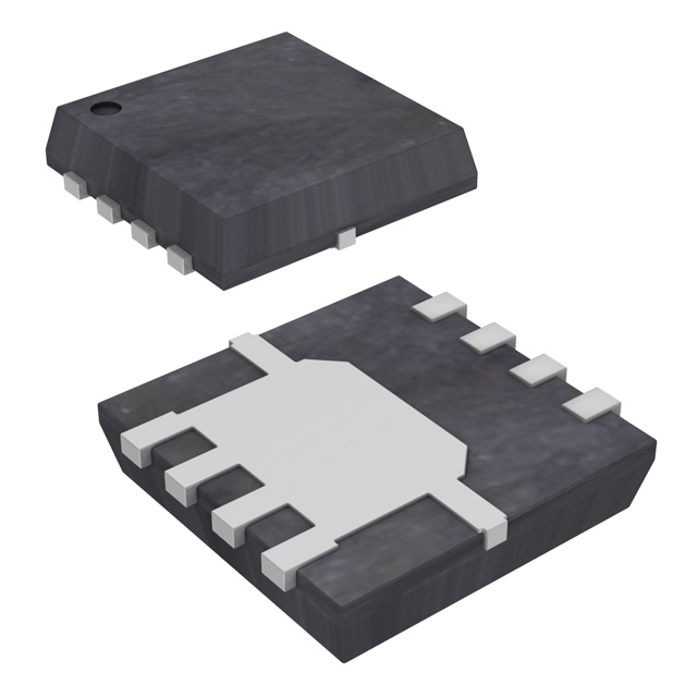
Single N-Channel Power MOSFET 30V, 23A, 23mΩ, WDFN8 3.3x3.3, 0.65P, 5000-REEL
Why Choose Us?
Professional Platform
B2B & B2C purchasingDelivery at full speed
1-2 days deliveryWide variety
Original manufacturers365 days guarantee
Responsible quality
.png)


Tech Specifications
Continuous Drain Current (ID)
23A
Drain to Source Breakdown Voltage
30V
Drain to Source Resistance
30mR
Element Configuration
Single
Fall Time
3.6ns
Gate to Source Voltage (Vgs)
20V
Input Capacitance
476pF
Lead Free
Lead Free
NTTFS4930NTWG Description
N-Channel 30 V 4.5A (Ta), 23A (Tc) 790mW (Ta), 20.2W (Tc) Surface Mount 8-WDFN (3.3x3.3)
FAQ
What is NTTFS4930NTWG?
NTTFS4930NTWG is a Single FETs, MOSFETs from onsemi. This product page provides its main specifications, pricing information, availability, and inquiry options.
What operating temperature range does NTTFS4930NTWG support?
What voltage specification is listed for NTTFS4930NTWG?
Is NTTFS4930NTWG currently in stock?
Are there related or alternative parts for NTTFS4930NTWG?
Quick Quote
ADD TO RFQ LIST
Not available to buy online? Want the lower wholesale price? Please Send RFQ to get best price, we will respond immediately
QUICK RFQ


.png?x-oss-process=image/format,webp/resize,h_32)


