onsemi
NVJS4151PT1G  
Single FETs, MOSFETs

onsemi
NVJS4151PT1G
278-NVJS4151PT1G
Ersa
onsemi-NVJS4151PT1G-datasheets-11658919.pdf
MOSFET P-CH 20V 3.2A SC88
In Stock : 29115

Not available to buy online? Want the lower wholesale price? Please Send RFQ to get best price, we will respond immediately

QUICK RFQ
ADD TO RFQ LIST
ersa FreeSample ersa flow
  • Quantity
  • Unit Price
  • Ext. Price
    • 1+
    • $0.29435
    • $0.29
    • 10+
    • $0.26786
    • $2.68
    • 30+
    • $0.25337
    • $7.6
    • 100+
    • $0.23681
    • $23.68
    • 500+
    • $0.21859
    • $109.3
    • 1000+
    • $0.21528
    • $215.28
    ADD TO CART
    QUICK ORDER
    $0.29435    $0.29
    ISO9001
    Quality Policy
    ISO45001
    ISO14001

    NVJS4151PT1G Description

    NVJS4151PT1G Description

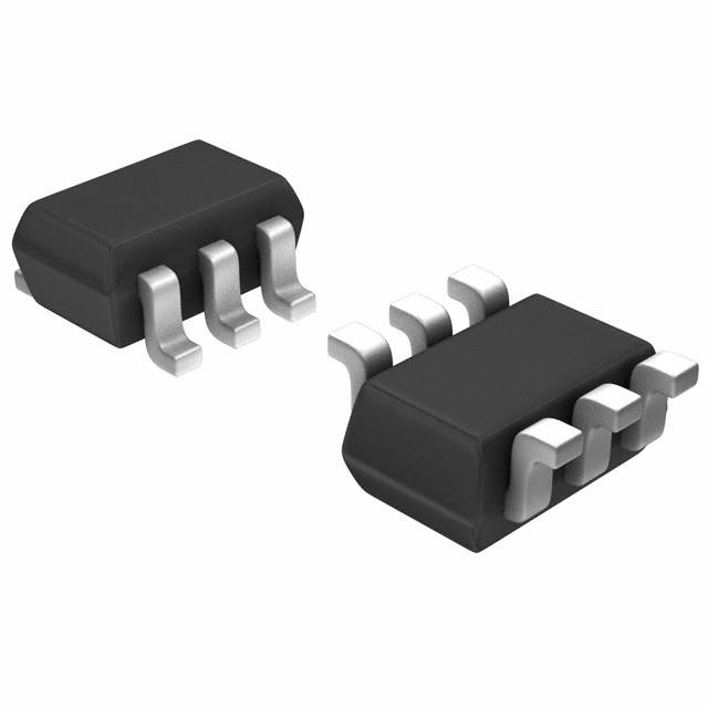
    The NVJS4151PT1G is a high-performance MOSFET (Metal Oxide) device from onsemi, designed for automotive applications. This P-Channel 20V, 3.2A SC88 MOSFET offers excellent electrical characteristics and reliability, making it suitable for a wide range of applications.

    NVJS4151PT1G Features

    • Input Capacitance (Ciss) (Max) @ Vds: 850 pF @ 10 V
    • Gate Charge (Qg) (Max) @ Vgs: 10 nC @ 4.5 V
    • Drain to Source Voltage (Vdss): 20 V
    • Power Dissipation (Max): 1.2W (Ta)
    • Rds On (Max) @ Id, Vgs: 67mOhm @ 2.9A, 4.5V
    • Vgs(th) (Max) @ Id: 1.2V @ 250µA
    • Current - Continuous Drain (Id) @ 25°C: 3.2A (Ta)
    • Drive Voltage (Max Rds On, Min Rds On): 1.5V, 4.5V
    • Moisture Sensitivity Level (MSL): 1 (Unlimited)
    • Mounting Type: Surface Mount
    • Package: Tape & Reel (TR)
    • Grade: Automotive
    • REACH Status: REACH Unaffected
    • RoHS Status: ROHS3 Compliant
    • ECCN: EAR99
    • HTSUS: 8541.29.0095

    The NVJS4151PT1G stands out from similar models due to its low Rds On, high input capacitance, and low gate charge, which contribute to improved efficiency and performance in high-frequency applications.

    NVJS4151PT1G Applications

    The NVJS4151PT1G is ideal for a variety of automotive and industrial applications where high efficiency, reliability, and performance are critical. Some specific use cases include:

    1. Power Management: In automotive systems, this MOSFET can be used for power management and control, providing efficient power distribution and regulation.
    2. Motor Control: The low Rds On and high current handling capabilities make it suitable for motor control applications, such as electric power steering and window lift systems.
    3. LED Lighting: In automotive lighting systems, the NVJS4151PT1G can be used for efficient LED driving and control, ensuring consistent brightness and color.
    4. Automotive Electronics: This MOSFET can be used in various automotive electronic systems, such as infotainment, climate control, and safety features.

    Conclusion of NVJS4151PT1G

    The NVJS4151PT1G is a robust and reliable MOSFET designed for automotive applications. Its unique features, such as low Rds On, high input capacitance, and low gate charge, make it an excellent choice for high-efficiency and high-performance applications. With its automotive-grade rating and compliance with REACH and RoHS regulations, the NVJS4151PT1G is a trusted solution for demanding automotive and industrial applications.

    Tech Specifications

    Unit Weight
    Configuration
    Package Name
    Input Capacitance (Ciss) (Max) @ Vds
    Gate Charge (Qg) (Max) @ Vgs
    PPAP
    OPN in older Technology
    Fall Time
    Automotive
    RoHS
    Maximum IDSS (uA)
    Typical Turn-On Delay Time
    Q gd Typ @ V GS = 4.5 V (nC)
    REACH Status
    Channel Type
    Wide SOA Mosfets
    Maximum Continuous Drain Current (A)
    MSL Temp (°C)
    Status
    Maximum Drain Source Voltage (V)
    Supplier Temperature Grade
    Rds On (Max) @ Id, Vgs
    Standard Package Name
    MSL Type
    Mounting
    C rss Typ (pF)
    Qualification
    Rise Time
    I d Max (A)
    Current - Continuous Drain (Id) @ 25°C
    Vgs th - Gate-Source Threshold Voltage
    Package
    P D Max (W)
    R DS(on) Max @ V GS = 4.5 V (mΩ)
    C oss Typ (pF)
    Qg - Gate Charge
    Power Dissipation (Max)
    Process Technology
    Package Height
    Vgs (Max)
    Maximum Operating Temperature
    Q g Typ @ V GS = 4.5 V (nC)
    RoHS Status
    Q rr Typ (nC)
    Silicon Family
    Transistor Polarity
    Minimum Operating Temperature
    Vds - Drain-Source Breakdown Voltage
    Type
    Part Status
    Maximum Gate Threshold Voltage (V)
    Package Width
    Q g Typ @ V GS = 10 V (nC)
    Typical Turn-Off Delay Time (ns)
    Maximum Gate Source Leakage Current (nA)
    Id - Continuous Drain Current
    V gs(th) Max (V)
    Typical Rise Time (ns)
    Channel Mode
    Typical Turn-On Delay Time (ns)
    Product Status
    Drain to Source Voltage (Vdss)
    Supplier Package
    Transistor Type
    Package / Case
    Number of Channels
    Technology
    EU RoHS
    Rds On - Drain-Source Resistance
    Moisture Sensitivity Level (MSL)
    Operating Temperature
    Channel Polarity
    Maximum Drain Source Resistance (mOhm)
    ECCN
    Grade
    V (BR)DSS Min (V)
    Mounting Type
    Vgs(th) (Max) @ Id
    Pin Count
    Drive Voltage (Max Rds On, Min Rds On)
    HTSUS
    USHTS
    Typical Gate Charge @ Vgs (nC)
    Typical Input Capacitance @ Vds (pF)
    Category
    Case Outline
    PCB changed
    HTS
    FET Type
    Number of Elements per Chip
    ECCN (US)
    Maximum Power Dissipation (mW)
    Gate Level
    Supplier Device Package
    Minimum Operating Temperature (°C)
    C iss Typ (pF)
    Maximum Operating Temperature (°C)
    Typical Fall Time (ns)
    V GS Max (V)
    Mfr
    Mounting Style
    R DS(on) Max @ V GS = 2.5 V (mΩ)
    FET Feature
    Maximum Gate Source Voltage (V)
    Vgs - Gate-Source Voltage
    Typical Turn-Off Delay Time
    Package Length
    Series
    Forward Transconductance - Min
    Pd - Power Dissipation
    Base Product Number

    NVJS4151PT1G Documents

    Download datasheets and manufacturer documentation for NVJS4151PT1G

    Ersa NVJS4151P      
    Ersa NVJS4151P      
    Ersa onsemi RoHS       onsemi REACH       Material Declaration NVJS4151PT1G      

    Shopping Guide

    Payment Methods
    Payment Methods include Prepayment TT (bank transfer), Western Union, and PayPal. Customers are responsible for shipping costs, bank charges, customs duties and taxes.
    Shipping Rate
    Shipments are made once a day around 5pm, excluding Sundays. Once shipped, the estimated delivery time is usually 5-7 business days, depending on the courier you choose.
    Delivery Methods
    Provide DHL, FedEx, UPS, EMS, SF Express and Registered Airmail International Delivery Service