
 German
 Japanese
 Portuguese
 Korea
Korea
 Mexico
 Dutch
Dutch


onsemi
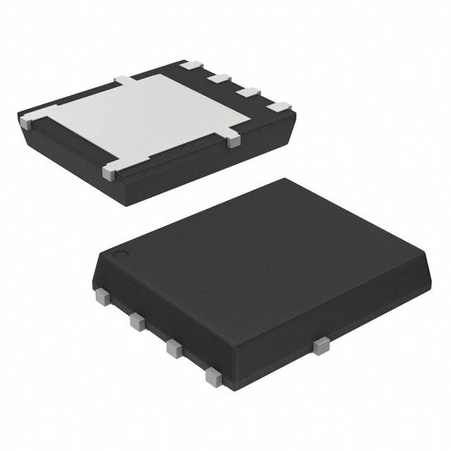
NVMFS5C628NLWFAFT1G

Why Choose Us?
Professional Platform
B2B & B2C purchasingDelivery at full speed
1-2 days deliveryWide variety
Original manufacturers365 days guarantee
Responsible quality
.png)


Tech Specifications
NVMFS5C628NLWFAFT1G Description
NVMFS5C628NLWFAFT1G Description
The NVMFS5C628NLWFAFT1G is a high-performance N-Channel MOSFET designed for automotive applications. Manufactured by onsemi, this MOSFET offers excellent electrical characteristics and robust performance in demanding environments. With a drain-to-source voltage of 60V and a continuous drain current of 28A at 25°C, this device is ideal for applications requiring high power handling and efficient switching.
NVMFS5C628NLWFAFT1G Features
- Technology: MOSFET (Metal Oxide)
- Grade: Automotive
- Mounting Type: Surface Mount, Wettable Flank
- Input Capacitance (Ciss) (Max) @ Vds: 3600 pF @ 25 V
- Gate Charge (Qg) (Max) @ Vgs: 52 nC @ 10 V
- Drain to Source Voltage (Vdss): 60 V
- Power Dissipation (Max): 3.7W (Ta), 110W (Tc)
- Rds On (Max) @ Id, Vgs: 2.4mOhm @ 50A, 10V
- Vgs(th) (Max) @ Id: 2V @ 135µA
- Current - Continuous Drain (Id) @ 25°C: 28A (Ta), 150A (Tc)
- Drive Voltage (Max Rds On, Min Rds On): 4.5V, 10V
- Vgs (Max): ±20V
- Moisture Sensitivity Level (MSL): 1 (Unlimited)
- REACH Status: REACH Unaffected
- RoHS Status: ROHS3 Compliant
- ECCN: EAR99
- HTSUS: 8541.29.0095
- Package: Tape & Reel (TR)
NVMFS5C628NLWFAFT1G Applications
The NVMFS5C628NLWFAFT1G is well-suited for various automotive applications, including:
- Battery Management Systems: Its high voltage and current ratings make it ideal for managing battery charging and discharging in electric and hybrid vehicles.
- Motor Control: The low Rds On and high current capability enable efficient motor control in applications such as electric power steering and window lifts.
- Power Supplies: The device's high power dissipation and robust performance make it suitable for automotive power supply systems, ensuring reliable operation under varying load conditions.
Conclusion of NVMFS5C628NLWFAFT1G
The NVMFS5C628NLWFAFT1G is a versatile and high-performance MOSFET designed for demanding automotive applications. Its unique combination of high voltage, current, and power ratings, along with its automotive-grade design, makes it an excellent choice for applications requiring efficient power management and control. With its robust performance and compliance with industry standards, the NVMFS5C628NLWFAFT1G is a reliable solution for automotive engineers looking to optimize their designs for performance and reliability.
FAQ
Not available to buy online? Want the lower wholesale price? Please Send RFQ to get best price, we will respond immediately


.png?x-oss-process=image/format,webp/resize,h_32)


