
 German
 Japanese
 Portuguese
 Korea
Korea
 Mexico
 Dutch
Dutch


onsemi
RFD16N05LSM9A
278-RFD16N05LSM9A

PDF Datasheet
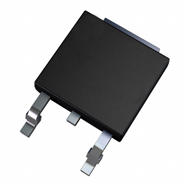
N-Channel Logic Level Power MOSFET 50V, 16A, 47mΩ, 2500-REEL
12 Weeks
Why Choose Us?
Professional Platform
B2B & B2C purchasingDelivery at full speed
1-2 days deliveryWide variety
Original manufacturers365 days guarantee
Responsible quality
.png)


Tech Specifications
Max Operating Temperature
150
Number of Terminals
2
Terminal Position
SINGLE
JEDEC Package Code
TO-252AA
Number of Elements
1
Eccn Code
EAR99
Lead Free
Yes
HTS Code
8541.29.00.95
RFD16N05LSM9A Description
N-Channel 50 V 16A (Tc) 60W (Tc) Surface Mount TO-252AA
FAQ
What is RFD16N05LSM9A?
RFD16N05LSM9A is a Single FETs, MOSFETs from onsemi. This product page provides its main specifications, pricing information, availability, and inquiry options.
Are there related or alternative parts for RFD16N05LSM9A?
What package or case is RFD16N05LSM9A available in?
Is RFD16N05LSM9A currently in stock?
What operating temperature range does RFD16N05LSM9A support?
Quick Quote
ADD TO RFQ LIST
Not available to buy online? Want the lower wholesale price? Please Send RFQ to get best price, we will respond immediately
QUICK RFQ


.png?x-oss-process=image/format,webp/resize,h_32)


