
 German
 Japanese
 Portuguese
 Korea
Korea
 Mexico
 Dutch
Dutch


Renesas Electronics Corporation
IDT74FCT3807APY8

Why Choose Us?
Professional Platform
B2B & B2C purchasingDelivery at full speed
1-2 days deliveryWide variety
Original manufacturers365 days guarantee
Responsible quality
.png)


Tech Specifications
IDT74FCT3807APY8 Description
IDT74FCT3807APY8 Description
The IDT74FCT3807APY8 is a high-performance clock buffer IC designed for applications requiring reliable and efficient signal distribution. Manufactured by Renesas Electronics Corporation, this device belongs to the 74FCT series and is specifically tailored for fanout buffer applications. It features a 1:10 input-to-output ratio, enabling it to distribute a single input clock signal to ten output signals with minimal propagation delay and skew. The IDT74FCT3807APY8 operates within a supply voltage range of 3V to 3.6V and supports LVTTL input and CMOS/TTL output, making it compatible with a wide range of digital systems.
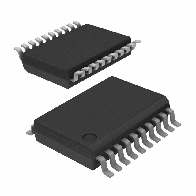
This IC is housed in a 20-pin SSOP (Shrink Small Outline Package) and is available in a surface-mount configuration, which is ideal for compact and high-density PCB designs. The operating temperature range of 0°C to 70°C ensures stable performance in various environmental conditions. Although the product is now obsolete, it remains a viable option for legacy systems and specific applications where its unique features are required.
IDT74FCT3807APY8 Features
- High Fanout Capability: The 1:10 input-to-output ratio allows for efficient distribution of clock signals, reducing the need for multiple buffer stages and simplifying circuit design.
- Wide Operating Voltage Range: The 3V to 3.6V supply voltage range ensures compatibility with a variety of power supply configurations, enhancing its versatility.
- Low Propagation Delay and Skew: The IDT74FCT3807APY8 is designed to minimize propagation delay and skew, ensuring that the distributed clock signals remain synchronized and accurate.
- LVTTL Input and CMOS/TTL Output: This combination of input and output standards provides compatibility with a broad range of digital systems, making it suitable for various applications.
- Surface-Mount Packaging: The 20-pin SSOP package and surface-mount configuration enable high-density PCB layouts, which is crucial for modern electronic designs.
- Wide Operating Temperature Range: The 0°C to 70°C operating temperature range ensures reliable performance in diverse environmental conditions.
- Moisture Sensitivity Level 1: The MSL 1 (Unlimited) rating indicates that the device is not sensitive to moisture, reducing the risk of damage during manufacturing and storage.
IDT74FCT3807APY8 Applications
The IDT74FCT3807APY8 is ideal for a variety of applications where efficient clock signal distribution is critical. Some specific use cases include:
- Computer Systems: Distributing clock signals to multiple components within a computer system, ensuring synchronized operation of processors, memory, and peripherals.
- Telecommunications: Providing reliable clock distribution in communication equipment, such as routers, switches, and base stations.
- Industrial Control Systems: Ensuring accurate timing and synchronization in industrial automation and control systems.
- Consumer Electronics: Used in devices such as televisions, gaming consoles, and other consumer electronics where precise clock signal distribution is necessary.
Conclusion of IDT74FCT3807APY8
The IDT74FCT3807APY8 is a robust and versatile clock buffer IC that offers significant advantages for applications requiring efficient clock signal distribution. Its high fanout capability, wide operating voltage range, and compatibility with various digital systems make it a reliable choice for a wide range of applications. Although now obsolete, the IDT74FCT3807APY8 remains a valuable component for legacy systems and specific use cases where its unique features are essential. For designers and engineers looking for a reliable clock distribution solution, the IDT74FCT3807APY8 is a proven and effective option.
FAQ
Not available to buy online? Want the lower wholesale price? Please Send RFQ to get best price, we will respond immediately


.png?x-oss-process=image/format,webp/resize,h_32)


