
 German
 Japanese
 Portuguese
 Korea
Korea
 Mexico
 Dutch
Dutch


Samsung Electro-Mechanics
RF062PJ200CS

Why Choose Us?
Professional Platform
B2B & B2C purchasingDelivery at full speed
1-2 days deliveryWide variety
Original manufacturers365 days guarantee
Responsible quality
.png)


Tech Specifications
RF062PJ200CS Description
RF062PJ200CS Description
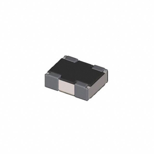
The RF062PJ200CS from Samsung Electro-Mechanics is a compact, high-performance 2-resistor array designed for surface-mount applications. Packaged in an 0302 (0805 Metric) case with long-side terminals, it features a 20Ω resistance per element with a ±5% tolerance and a ±200ppm/°C temperature coefficient. The ultra-low 0.013" (0.33mm) profile and miniature 0.031" x 0.024" (0.80mm x 0.60mm) footprint make it ideal for space-constrained PCB designs. With 31.25mW power dissipation per resistor, isolated circuit configuration, and RoHS3/REACH compliance, it meets stringent environmental and reliability standards.
RF062PJ200CS Features
- Dual-Resistor Array: Two isolated 20Ω resistors in a single package, reducing board space and assembly complexity.
- High-Density Design: Ultra-thin 0.33mm height and compact 0805 Metric footprint for dense layouts.
- Stable Performance: ±200ppm/°C TCR ensures consistent resistance across temperature variations.
- Robust Construction: MSL 1 (Unlimited) moisture sensitivity and flat terminals for reliable soldering.
- Industry Compliance: RoHS3, REACH, and ECCN EAR99 certified for global use.
RF062PJ200CS Applications
This resistor array excels in high-frequency circuits, signal termination, and impedance matching due to its low parasitic effects. Its miniature size suits wearables, IoT devices, and mobile electronics, while the isolated design is optimal for sensor interfaces, ADC/DAC circuits, and voltage dividers. The tape-and-reel packaging enables efficient automated pick-and-place assembly in volume production.
Conclusion of RF062PJ200CS
The RF062PJ200CS combines miniaturization, precision, and reliability, making it a superior choice for modern electronics. Its dual-resistor isolation, low-profile form factor, and compliance with environmental standards address critical needs in consumer, industrial, and telecom applications. Engineers benefit from reduced BOM complexity and enhanced signal integrity, solidifying its role in next-generation PCB designs.
FAQ
Not available to buy online? Want the lower wholesale price? Please Send RFQ to get best price, we will respond immediately


.png?x-oss-process=image/format,webp/resize,h_32)


