

STMicroelectronics
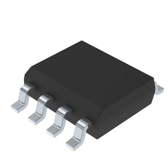
LF351DT
OP Amps, Buffer Amps ICs
Not available to buy online? Want the lower wholesale price? Please Send RFQ to get best price, we will respond immediately


.png?x-oss-process=image/format,webp/resize,p_30)


LF351DT Description
LF351DT Description
The LF351DT is an operational amplifier (op-amp) from STMicroelectronics, designed for high performance in a variety of applications. This device is part of the LF351 family, which is known for its JFET input stage, providing excellent input offset voltage and drift performance. With a supply voltage range from 6V to 32V, the LF351DT is suitable for a wide range of power supply configurations. It is currently an active product, compliant with the REACH regulations and RoHS3 standards, ensuring environmental and health safety.
LF351DT Features
- Voltage - Supply Span: The LF351DT can operate with a supply voltage ranging from 6V to 32V, offering flexibility in power supply design.
- Gain Bandwidth Product: With a gain bandwidth product of 4 MHz, this op-amp is suitable for applications requiring high-speed amplification.
- Slew Rate: A fast slew rate of 16V/µs ensures quick response to input signal changes, making it ideal for high-frequency applications.
- Current - Input Bias: The ultra-low input bias current of 20 pA minimizes power consumption and improves stability in high-impedance circuits.
- Current - Supply: Consuming only 1.4mA, the LF351DT is energy-efficient, suitable for battery-powered devices.
- Voltage - Input Offset: A low input offset voltage of 3 mV contributes to high accuracy in signal processing.
- Operating Temperature: The LF351DT operates within a wide temperature range of 0°C to 70°C, making it suitable for both indoor and outdoor applications.
- Mounting Type: Surface mount packaging allows for compact and efficient PCB layout.
LF351DT Applications
The LF351DT's combination of high performance and low power consumption makes it ideal for a variety of applications, including:
- Audio Amplification: Its low noise and high slew rate make it suitable for audio preamplifiers and line drivers.
- Sensor Conditioning: The low input offset voltage and drift are beneficial for accurate sensor signal conditioning in industrial applications.
- Data Acquisition Systems: The LF351DT's high-speed performance is well-suited for data acquisition systems requiring fast signal processing.
- Medical Equipment: Due to its low noise and precision, it can be used in medical equipment for signal amplification and processing.
Conclusion of LF351DT
The LF351DT from STMicroelectronics is a high-performance operational amplifier that stands out due to its JFET input stage, offering superior input offset voltage and drift performance. Its wide supply voltage range, low power consumption, and fast slew rate make it a versatile choice for various applications, from audio amplification to sensor conditioning. The LF351DT's compliance with REACH and RoHS3 standards, along with its robust performance characteristics, position it as a reliable option for demanding electronics applications.
Tech Specifications
LF351DT Documents
Download datasheets and manufacturer documentation for LF351DT
 PROCESS CHANGE NOTIFICATION (PDF) Product Change Notification (PDF) PRODUCT / PROCESS CHANGE INFORMATION (PDF) LF351DT Symbol & Footprint by SnapMagic
 Related Parts


Shopping Guide


.png?x-oss-process=image/format,webp/resize,h_32)


©2025 ERSA Electronics Corporation.