
 German
 Japanese
 Portuguese
 Korea
Korea
 Mexico
 Dutch
Dutch


STMicroelectronics
STE53NC50
Why Choose Us?
Professional Platform
B2B & B2C purchasingDelivery at full speed
1-2 days deliveryWide variety
Original manufacturers365 days guarantee
Responsible quality
.png)


Tech Specifications
STE53NC50 Description
STE53NC50 Description
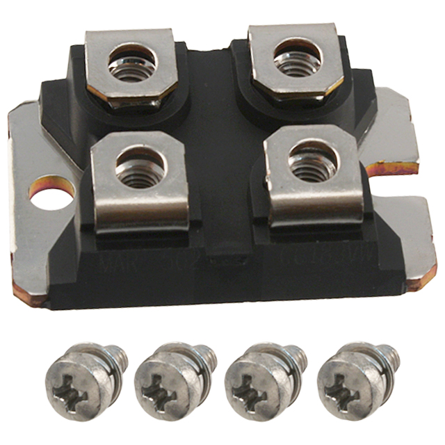
The STE53NC50 is a high-performance N-Channel MOSFET from STMicroelectronics, designed for demanding power management applications. With its robust 500V drain-to-source voltage rating and a continuous drain current of 53A at 25°C, this device delivers exceptional performance in a compact ISOTOP package. The STE53NC50 is engineered with advanced MOSFET technology, ensuring high efficiency and reliability in various electronic systems.
STE53NC50 Features
- High Voltage Rating: The STE53NC50 boasts a 500V drain-to-source voltage, making it suitable for high-voltage applications.
- High Current Capacity: Capable of handling 53A continuous drain current at 25°C, this MOSFET is ideal for power-intensive applications.
- Low On-Resistance: With an Rds(on) of just 80mOhm at 27A and 10V, the STE53NC50 minimizes power losses and enhances efficiency.
- Advanced MOSFET Technology: Utilizing PowerMESH™ II technology, this device offers superior performance and reliability.
- Robust Package: The ISOTOP package provides excellent thermal management and mechanical stability.
- Compliance: The STE53NC50 is REACH unaffected and RoHS3 compliant, ensuring environmental and regulatory compliance.
STE53NC50 Applications
The STE53NC50 is well-suited for a variety of applications where high voltage and current handling are required:
- Industrial Control Systems: Its high voltage and current ratings make it ideal for motor drives and power supplies in industrial settings.
- Automotive Applications: The robustness of the STE53NC50 makes it suitable for automotive power management systems, such as battery chargers and inverters.
- Renewable Energy Systems: In solar and wind power systems, the STE53NC50 can efficiently manage power conversion and distribution.
- Telecommunications: For power supplies in telecommunications equipment, the STE53NC50 provides reliable performance and high efficiency.
Conclusion of STE53NC50
The STE53NC50 from STMicroelectronics is a powerful and versatile N-Channel MOSFET, offering a combination of high voltage and current ratings with advanced technology. Its unique features, such as low on-resistance and a robust ISOTOP package, make it an excellent choice for demanding applications in industrial control, automotive, renewable energy, and telecommunications. With its compliance with REACH and RoHS standards, the STE53NC50 is not only a high-performance device but also an environmentally responsible choice.
FAQ
| Quantity | Unit Price | Ext. Price |
|---|---|---|
| 1+ | $51.82457 | $51.82 |
| 30+ | $49.45715 | $1483.71 |
Not available to buy online? Want the lower wholesale price? Please Send RFQ to get best price, we will respond immediately


.png?x-oss-process=image/format,webp/resize,h_32)


