

STMicroelectronics
STG5682QTR
Analog Switches, Multiplexers, Demultiplexers

Not available to buy online? Want the lower wholesale price? Please Send RFQ to get best price, we will respond immediately


.png?x-oss-process=image/format,webp/resize,p_30)


STG5682QTR Description
STG5682QTR Description
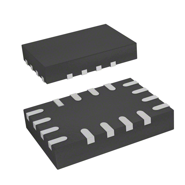
The STG5682QTR is a high-performance analog switch from STMicroelectronics, designed to meet the demands of modern electronic systems. This 2:1 multiplexer/demultiplexer is housed in a compact 16-QFN package, making it ideal for space-constrained applications. With its low on-state resistance of 550mOhm and a -3dB bandwidth of 33MHz, the STG5682QTR offers excellent signal integrity and fast switching capabilities.
STG5682QTR Features
- Low On-State Resistance: The STG5682QTR boasts an on-state resistance of just 550mOhm, ensuring minimal signal loss and distortion.
- Fast Switching: With a maximum switch time of 80ns for Ton and 50ns for Toff, the STG5682QTR provides rapid signal routing.
- Low Charge Injection: At 126pC, the STG5682QTR minimizes the impact of charge injection, preserving signal integrity.
- Channel-to-Channel Matching: The STG5682QTR offers excellent channel-to-channel matching with a maximum ΔRon of 15mOhm, ensuring consistent performance across channels.
- Low Leakage Current: The STG5682QTR has a maximum leakage current of 100nA, reducing power consumption in standby modes.
- Wide Voltage Range: The device operates over a supply voltage range of 1.65V to 4.5V, making it suitable for a variety of applications.
- REACH and RoHS Compliance: The STG5682QTR is REACH unaffected and RoHS3 compliant, ensuring environmental and regulatory compliance.
STG5682QTR Applications
The STG5682QTR is ideal for a range of applications where signal integrity, fast switching, and low power consumption are critical:
- Audio and Video Processing: The STG5682QTR's low distortion and fast switching make it suitable for audio and video signal routing in consumer electronics.
- Automotive Electronics: In automotive applications, the STG5682QTR can be used for signal multiplexing in infotainment systems and sensor interfaces.
- Industrial Control Systems: The STG5682QTR's robust performance and wide voltage range make it suitable for use in industrial control systems, where signal integrity and reliability are paramount.
- Medical Devices: In medical devices, the STG5682QTR can be used for signal routing and multiplexing in imaging systems and patient monitoring equipment.
Conclusion of STG5682QTR
The STG5682QTR from STMicroelectronics is a versatile and high-performance 2:1 multiplexer/demultiplexer, offering a combination of low on-state resistance, fast switching, and excellent signal integrity. Its compact form factor, wide voltage range, and compliance with REACH and RoHS standards make it an ideal choice for a variety of applications in the audio, video, automotive, industrial, and medical sectors. With its unique features and advantages, the STG5682QTR stands out as a reliable and efficient solution for signal routing and multiplexing in demanding electronic systems.
Tech Specifications
STG5682QTR Documents
Download datasheets and manufacturer documentation for STG5682QTR
STG5682 Moisture Barrier Bag 09/May/2016 STG5682 View All Specifications STG5682 Related Parts


Shopping Guide


.png?x-oss-process=image/format,webp/resize,h_32)


©2025 ERSA Electronics Corporation.