
 German
 Japanese
 Portuguese
 Korea
Korea
 Mexico
 Dutch
Dutch


STMicroelectronics
STW70N65DM6
278-STW70N65DM6

PDF Datasheet
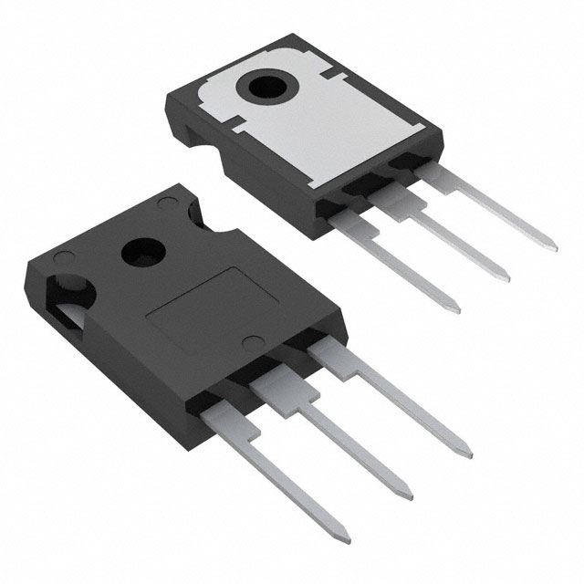
N-channel 650 V, 36 mOhm typ., 68 A MDmesh DM6 Power MOSFET in a TO-247 package
18 Weeks
Why Choose Us?
Professional Platform
B2B & B2C purchasingDelivery at full speed
1-2 days deliveryWide variety
Original manufacturers365 days guarantee
Responsible quality
.png)


Tech Specifications
RoHS
Yes
REACH
not_compliant
Military Spec
False
STW70N65DM6 Description
N-Channel 650 V 68A (Tc) 450W (Tc) Through Hole TO-247-3
FAQ
What is STW70N65DM6?
STW70N65DM6 is a Single FETs, MOSFETs from STMicroelectronics. This product page provides its main specifications, pricing information, availability, and inquiry options.
Is STW70N65DM6 currently in stock?
Does STW70N65DM6 have quantity-based pricing?
What is the standard lead time for STW70N65DM6?
Are there related or alternative parts for STW70N65DM6?
Availability
(In Stock :
13 )
| Quantity | Unit Price | Ext. Price |
|---|---|---|
| 1+ | $30.37372 | $30.37 |
| 30+ | $28.81715 | $864.51 |
ADD TO CART
QUICK ORDER
Unit Price $30.37372
Subtotal $30.37
Quick Quote
ADD TO RFQ LIST
Not available to buy online? Want the lower wholesale price? Please Send RFQ to get best price, we will respond immediately
QUICK RFQ


.png?x-oss-process=image/format,webp/resize,h_32)


