STMicroelectronics_TL064CDT

STMicroelectronics
TL064CDT  
OP Amps, Buffer Amps ICs

STMicroelectronics
TL064CDT
687-TL064CDT
IC OPAMP JFET 4 CIRCUIT 14SO
In Stock : 7168

Not available to buy online? Want the lower wholesale price? Please Send RFQ to get best price, we will respond immediately

QUICK RFQ
ADD TO RFQ LIST
ersa FreeSample ersa flow
  • Quantity
  • Unit Price
  • Ext. Price
    • 5+
    • $0.24610
    • $1.23
    • 50+
    • $0.19531
    • $9.77
    • 150+
    • $0.17353
    • $26.03
    • 500+
    • $0.14637
    • $73.19
    • 2500+
    • $0.13427
    • $335.68
    • 5000+
    • $0.12702
    • $635.1
    ADD TO CART
    QUICK ORDER
    $0.00000    $0.00
    ISO9001
    Quality Policy
    ISO45001
    ISO14001

    TL064CDT Description

    The TL064CDT is a quad operational amplifier (op-amp) manufactured by STMicroelectronics. It is a high-performance, low-power, JFET input operational amplifier that is designed for a wide range of applications.

    Description:

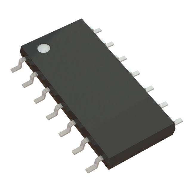
    The TL064CDT is a 14-pin DIP (Dual In-line Package) integrated circuit that consists of four independent operational amplifiers. Each op-amp has high input impedance, low input offset voltage, and low output noise characteristics. The device is specified over a wide supply voltage range of ±3V to ±18V and operates over a temperature range of -40°C to +125°C.

    Features:

    1. JFET input stage for high input impedance and low input offset voltage.
    2. Low input bias and offset currents.
    3. Wide supply voltage range: ±3V to ±18V.
    4. Low output noise.
    5. Short-circuit protection.
    6. High common-mode and differential voltage range.
    7. Internal frequency compensation.
    8. Available in 14-pin DIP package.

    Applications:

    The TL064CDT is suitable for a variety of applications due to its high input impedance, low input offset voltage, and low output noise characteristics. Some of the common applications include:

    1. Audio preamplifiers and buffers.
    2. DC and AC amplifiers.
    3. Signal conditioning circuits.
    4. Strain gauge and temperature sensor amplifiers.
    5. In instrumentation and process control systems.
    6. Medical equipment.
    7. Active filters and equalizers.
    8. Oscillators and waveform generators.

    The TL064CDT's versatility and performance make it a popular choice for a wide range of analog signal processing applications.

    Tech Specifications

    Voltage - Supply Span (Max)
    Number of Channels per Chip
    Power Supply Type
    Maximum Input Offset Voltage (mV)
    PPAP
    Gain Bandwidth Product
    Product Status
    Current - Input Bias
    Automotive
    Maximum Input Offset Current (uA)
    Supplier Package
    Package / Case
    Typical Voltage Gain (dB)
    REACH Status
    EU RoHS
    Amplifier Type
    Maximum Dual Supply Voltage (V)
    Moisture Sensitivity Level (MSL)
    Typical Input Noise Voltage Density (nV/rtHz)
    Operating Temperature
    Typical Slew Rate (V/us)
    ECCN
    Mounting Type
    Current - Supply
    Standard Package Name
    Pin Count
    Shut Down Support
    Mounting
    Typical Dual Supply Voltage (V)
    Voltage - Supply Span (Min)
    Lead Shape
    Manufacturer Type
    HTSUS
    Package
    Current - Output / Channel
    Minimum CMRR (dB)
    Maximum Quiescent Current (mA)
    PCB changed
    Output Type
    HTS
    ECCN (US)
    Maximum Power Dissipation (mW)
    Supplier Device Package
    Minimum CMRR Range (dB)
    Minimum Operating Temperature (°C)
    Maximum Operating Temperature (°C)
    Process Technology
    Typical Gain Bandwidth Product (MHz)
    Package Height
    Mfr
    RoHS Status
    Maximum Input Bias Current (uA)
    Slew Rate
    Package Length
    Minimum Dual Supply Voltage (V)
    Voltage - Input Offset
    Series
    Type
    Part Status
    Number of Circuits
    Package Width
    Base Product Number
    Maximum Dual Supply Voltage
    Unit Weight
    en - Input Voltage Noise Density
    Vos - Input Offset Voltage
    Voltage Gain dB
    Dual Supply Voltage
    Minimum Dual Supply Voltage
    Product
    RoHS
    Supply Voltage - Min
    Operating Supply Current
    SR - Slew Rate
    Number of Channels
    Technology
    Height
    Maximum Operating Temperature
    Ib - Input Bias Current
    Supply Voltage - Max
    Width
    Mounting Style
    PSRR - Power Supply Rejection Ratio
    Minimum Operating Temperature
    CMRR - Common Mode Rejection Ratio
    Shutdown
    Length
    Operating Supply Voltage
    Output Current per Channel
    Supply Type
    Pd - Power Dissipation
    USHTS
    GBP - Gain Bandwidth Product

    TL064CDT Documents

    Download datasheets and manufacturer documentation for TL064CDT

    Ersa TL064      
    Ersa Moisture Barrier Bag 09/May/2016      
    Ersa TL064 View All Specifications      
    Ersa TL064      

    Shopping Guide

    Payment Methods
    Payment Methods include Prepayment TT (bank transfer), Western Union, and PayPal. Customers are responsible for shipping costs, bank charges, customs duties and taxes.
    Shipping Rate
    Shipments are made once a day around 5pm, excluding Sundays. Once shipped, the estimated delivery time is usually 5-7 business days, depending on the courier you choose.
    Delivery Methods
    Provide DHL, FedEx, UPS, EMS, SF Express and Registered Airmail International Delivery Service