
STMicroelectronics
TS271CDT
OP Amps, Buffer Amps ICs


.png?x-oss-process=image/format,webp/resize,p_30)


TS271CDT Description
TS271CDT Description
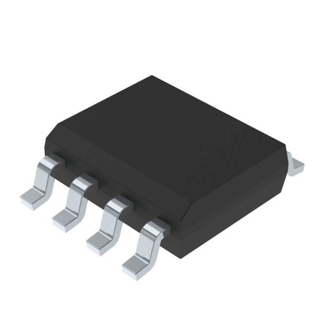
The TS271CDT is a high-performance operational amplifier (op-amp) from STMicroelectronics, designed for a wide range of applications in the electronics industry. This general-purpose op-amp offers excellent technical specifications and performance benefits, making it an ideal choice for various applications.
TS271CDT Features
- Voltage Supply Span: The TS271CDT operates over a wide voltage range, from 3 V to 16 V, providing flexibility in power supply requirements.
- Gain Bandwidth Product: With a gain bandwidth product of 100 kHz, this op-amp delivers high-speed performance for demanding applications.
- Input Bias Current: The ultra-low input bias current of 1 pA ensures minimal loading on input sources, maintaining signal integrity.
- Slew Rate: A fast slew rate of 0.04 V/µs enables rapid response to input signal changes, making it suitable for high-speed applications.
- Operating Temperature: The TS271CDT can operate in a wide temperature range of 0°C to 70°C, making it suitable for both commercial and industrial applications.
- Mounting Type: The surface-mount packaging allows for easy integration into PCB designs, reducing footprint and improving reliability.
- Current Supply: The low supply current of 10 µA contributes to low power consumption, making it ideal for battery-operated devices.
- Input Offset Voltage: The low input offset voltage of 1.1 mV ensures high accuracy and stability in signal amplification.
- RoHS Compliance: The TS271CDT is compliant with RoHS3 regulations, making it an environmentally friendly choice.
TS271CDT Applications
The TS271CDT is ideal for various applications due to its excellent technical specifications and performance benefits. Some specific use cases include:
- Audio Amplification: The low noise and high slew rate make it suitable for audio applications, such as preamplifiers and headphone amplifiers.
- Sensor Signal Conditioning: The low input bias current and wide supply voltage range make it ideal for conditioning signals from sensors in industrial and automotive applications.
- Data Acquisition Systems: The high slew rate and low input offset voltage make it suitable for data acquisition systems in test and measurement equipment.
- Battery-Powered Devices: The low power consumption and wide operating temperature range make it ideal for battery-operated devices, such as portable electronics and wearables.
Conclusion of TS271CDT
The TS271CDT is a versatile and high-performance op-amp from STMicroelectronics, offering excellent technical specifications and performance benefits. Its wide voltage supply span, low input bias current, and high slew rate make it an ideal choice for a variety of applications, including audio amplification, sensor signal conditioning, data acquisition systems, and battery-powered devices. With its RoHS compliance and surface-mount packaging, the TS271CDT is a reliable and environmentally friendly solution for your electronic design needs.
Tech Specifications
TS271CDT Documents
Download datasheets and manufacturer documentation for TS271CDT
 PROCESS CHANGE NOTIFICATION (PDF) Product / Process Change Notification (PDF) PRODUCT / PROCESS CHANGE INFORMATION (PDF)
 Shopping Guide


.png?x-oss-process=image/format,webp/resize,h_32)


