

STMicroelectronics
TS272CDT
OP Amps, Buffer Amps ICs
Not available to buy online? Want the lower wholesale price? Please Send RFQ to get best price, we will respond immediately


.png?x-oss-process=image/format,webp/resize,p_30)


TS272CDT Description
TS272CDT Description
The TS272CDT is a high-performance, dual operational amplifier (op-amp) integrated circuit (IC) from STMicroelectronics, designed to deliver exceptional performance in a wide range of applications. This CMOS op-amp features a gain bandwidth product of 3.5 MHz, a slew rate of 5.5 V/µs, and an input bias current of just 1 pA, making it ideal for applications requiring high-speed signal processing and low noise.
TS272CDT Features
- Voltage Supply Span: The TS272CDT operates over a wide voltage range of 3 V to 16 V, providing flexibility in power supply design.
- Low Input Bias Current: With an input bias current of just 1 pA, the TS272CDT minimizes power consumption and reduces noise in sensitive applications.
- High Slew Rate: The 5.5 V/µs slew rate enables the op-amp to handle fast-changing input signals, making it suitable for high-speed applications.
- Low Voltage Input Offset: At 1.1 mV, the low input offset voltage ensures accurate signal processing.
- Dual Circuit Design: The TS272CDT features two independent op-amps in a single package, providing flexibility in circuit design and reducing component count.
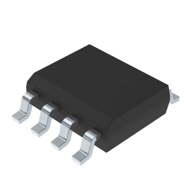
- Surface Mount Packaging: The TS272CDT is available in an 8-pin SOIC package, suitable for surface-mount applications and PCB design.
- RoHS Compliance: The TS272CDT is compliant with the RoHS3 directive, making it suitable for environmentally friendly electronics manufacturing.
TS272CDT Applications
The TS272CDT is ideal for a wide range of applications, including:
- Audio Amplification: The low noise and high slew rate make it suitable for audio signal processing in consumer electronics.
- Data Acquisition Systems: The high-speed performance and low input bias current are ideal for data acquisition systems in industrial and scientific applications.
- Sensor Signal Conditioning: The TS272CDT can be used to amplify and filter signals from sensors in IoT devices and industrial control systems.
- Medical Equipment: The low noise and high accuracy make it suitable for signal processing in medical equipment, such as ECG monitors and patient monitoring systems.
Conclusion of TS272CDT
The TS272CDT is a versatile and high-performance dual op-amp from STMicroelectronics, offering a combination of low noise, high speed, and flexibility in power supply design. Its unique features, such as low input bias current and high slew rate, make it an ideal choice for a wide range of applications, from audio amplification to sensor signal conditioning. With its RoHS compliance and surface-mount packaging, the TS272CDT is a reliable and environmentally friendly solution for modern electronics design.
Tech Specifications
TS272CDT Documents
Download datasheets and manufacturer documentation for TS272CDT
 TS272C,I,M TS272 View All Specifications TS272C,I,M
 Related Parts


Shopping Guide


.png?x-oss-process=image/format,webp/resize,h_32)


©2025 ERSA Electronics Corporation.