
STMicroelectronics
TS514IDT
OP Amps, Buffer Amps ICs


.png?x-oss-process=image/format,webp/resize,p_30)


TS514IDT Description
TS514IDT Description
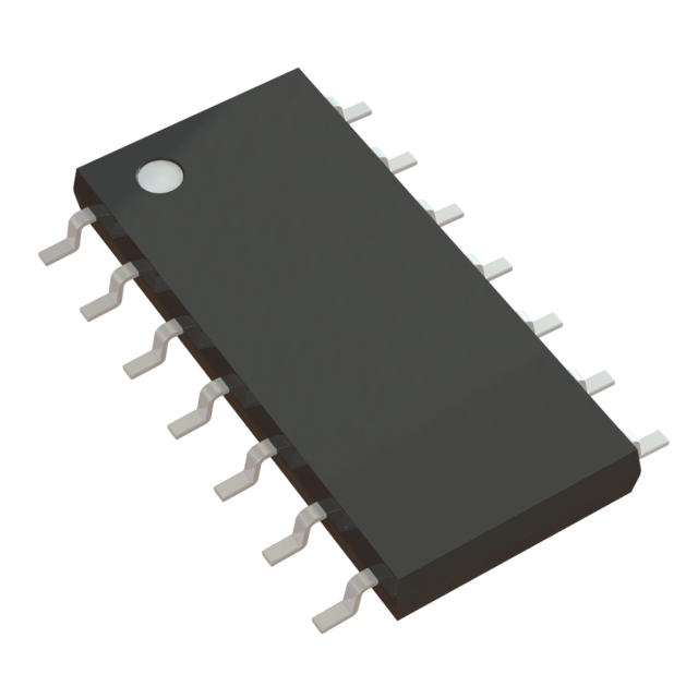
The TS514IDT is a high-performance, general-purpose operational amplifier (op-amp) from STMicroelectronics, designed for a wide range of applications requiring precision and reliability. This quad op-amp features a supply voltage range of 6 V to 30 V, making it suitable for both low-voltage and high-voltage applications. With a gain bandwidth product of 3 MHz and a slew rate of 1.5 V/µs, the TS514IDT ensures fast response times and accurate signal processing. The device is REACH unaffected and RoHS3 compliant, adhering to stringent environmental regulations and ensuring safe usage in various industries.
TS514IDT Features
- Wide Supply Voltage Range: The TS514IDT operates within a supply voltage span of 6 V to 30 V, providing flexibility for diverse power supply requirements.
- High Gain Bandwidth Product: With a gain bandwidth product of 3 MHz, the TS514IDT delivers high-frequency performance, making it ideal for applications requiring fast signal processing.
- Low Input Bias Current: The low input bias current of 50 nA ensures minimal loading on the input signal source, preserving signal integrity.
- Low Input Offset Voltage: The low input offset voltage of 500 µV guarantees accurate signal amplification, reducing errors in precision applications.
- High Output Current: Each channel can provide up to 23 mA of output current, enabling the TS514IDT to drive heavy loads effectively.
- Low Power Consumption: The device consumes only 500 µA of supply current, making it energy-efficient and suitable for battery-powered applications.
- Surface Mount Packaging: The TS514IDT is available in a surface mount package, facilitating easy integration into compact and high-density PCB designs.
- Moisture Sensitivity Level (MSL) 1: The TS514IDT has an MSL of 1, indicating unlimited exposure to moisture, which enhances its reliability in various environmental conditions.
TS514IDT Applications
The TS514IDT is well-suited for a variety of applications due to its versatile performance characteristics:
- Signal Conditioning: Ideal for amplifying and conditioning weak signals in sensor interfaces, ensuring accurate and reliable data transmission.
- Analog Filters: The high gain bandwidth product and low input offset voltage make the TS514IDT suitable for designing active filters with precise frequency response.
- Transimpedance Amplifiers: The low input bias current and high output current capability enable efficient conversion of current to voltage in photodiode and other current-based sensor applications.
- Power Management: The wide supply voltage range and low power consumption make the TS514IDT suitable for power management circuits in portable and battery-operated devices.
- Audio Processing: The TS514IDT can be used in audio signal processing applications, providing high-fidelity amplification and minimal distortion.
Conclusion of TS514IDT
The TS514IDT from STMicroelectronics stands out as a robust and versatile general-purpose operational amplifier. Its wide supply voltage range, high gain bandwidth product, and low power consumption make it an excellent choice for a variety of applications, from signal conditioning to power management. The low input bias current and input offset voltage ensure high precision and accuracy, while the high output current capability allows for effective load driving. With its surface mount packaging and compliance with environmental regulations, the TS514IDT offers a reliable and efficient solution for modern electronic designs.
Tech Specifications
TS514IDT Documents
Download datasheets and manufacturer documentation for TS514IDT
 PRODUCT / PROCESS CHANGE INFORMATION (PDF)
 Shopping Guide


.png?x-oss-process=image/format,webp/resize,h_32)


