

STMicroelectronics
TSB712IDT
OP Amps, Buffer Amps ICs

Not available to buy online? Want the lower wholesale price? Please Send RFQ to get best price, we will respond immediately


.png?x-oss-process=image/format,webp/resize,p_30)


TSB712IDT Description
TSB712IDT Description
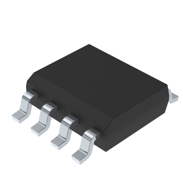
The TSB712IDT is a high-performance, general-purpose operational amplifier designed for a wide range of applications. Manufactured by STMicroelectronics, this device is part of the TSB712 series and is specifically tailored for automotive-grade use. The TSB712IDT features a dual-circuit configuration in an 8-pin SOIC package, making it suitable for surface-mount applications. It operates within a supply voltage range of 2.7 V to 36 V, providing flexibility for various power supply requirements. With a gain bandwidth product of 6 MHz and a slew rate of 3 V/µs, the TSB712IDT ensures high-speed signal processing and accurate amplification. The device also boasts a low input bias current of 300 nA and an input offset voltage of 1.2 mV, contributing to its precision and stability. The TSB712IDT is REACH unaffected and RoHS3 compliant, ensuring environmental safety and regulatory compliance. Its moisture sensitivity level is MSL 1 (unlimited), making it robust for various environmental conditions.
TSB712IDT Features
- Wide Supply Voltage Range: Operates from 2.7 V to 36 V, offering versatility for different power supply configurations.
- High Gain Bandwidth Product: 6 MHz ensures high-speed performance and accurate signal processing.
- Low Input Bias Current: 300 nA minimizes the impact on the input signal, enhancing precision.
- Low Input Offset Voltage: 1.2 mV ensures accurate amplification and minimal error in signal processing.
- High Slew Rate: 3 V/µs allows for fast response times and accurate reproduction of high-frequency signals.
- Dual-Circuit Configuration: Two operational amplifiers in a single package provide compact and efficient design solutions.
- Automotive Grade: Suitable for demanding automotive applications, ensuring reliability and performance.
- Surface Mount Packaging: 8-pin SOIC package is ideal for space-constrained designs and automated assembly processes.
- Environmental Compliance: REACH unaffected and RoHS3 compliant, ensuring safety and regulatory adherence.
- Moisture Sensitivity Level: MSL 1 (unlimited) makes it robust against environmental moisture.
TSB712IDT Applications
The TSB712IDT is ideal for a variety of applications, particularly in the automotive sector, where reliability and performance are paramount. Its wide supply voltage range and high gain bandwidth product make it suitable for:
- Signal Conditioning: Amplifying and conditioning signals in automotive sensors and control systems.
- Power Management: Managing power in automotive electronic control units (ECUs) and infotainment systems.
- Audio Processing: Enhancing audio quality in automotive sound systems.
- Industrial Control: Controlling and monitoring industrial processes where precision and speed are critical.
- Consumer Electronics: Amplifying signals in various consumer devices, such as portable audio equipment and smart home devices.
Conclusion of TSB712IDT
The TSB712IDT from STMicroelectronics is a versatile and high-performance operational amplifier designed for automotive and industrial applications. Its wide supply voltage range, high gain bandwidth product, and low input bias current make it an excellent choice for demanding environments. The dual-circuit configuration in a compact 8-pin SOIC package ensures efficient and space-saving design solutions. With its automotive-grade reliability, environmental compliance, and robustness against moisture, the TSB712IDT stands out as a reliable and high-performance solution for a wide range of applications.
Tech Specifications
TSB712IDT Documents
Download datasheets and manufacturer documentation for TSB712IDT
Product Change Notification (PDF) Related Parts


Shopping Guide


.png?x-oss-process=image/format,webp/resize,h_32)


©2025 ERSA Electronics Corporation.