
 German
 Japanese
 Portuguese
 Korea
Korea
 Mexico
 Dutch
Dutch


STMicroelectronics
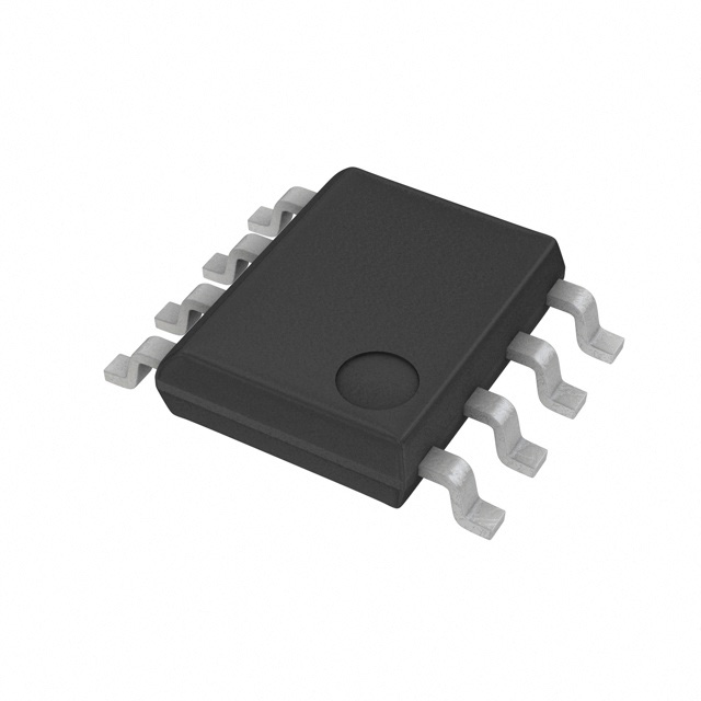
TSB7192AIST

Why Choose Us?
Professional Platform
B2B & B2C purchasingDelivery at full speed
1-2 days deliveryWide variety
Original manufacturers365 days guarantee
Responsible quality
.png)


Tech Specifications
TSB7192AIST Description
TSB7192AIST Description
The TSB7192AIST is a high-performance, general-purpose operational amplifier designed for a wide range of applications. Manufactured by STMicroelectronics, this IC is part of the Linear IC Chips category and is specifically tailored for automotive-grade use. The TSB7192AIST features a dual-circuit configuration, offering flexibility and efficiency in various electronic systems. With a supply voltage range of 2.7 V to 36 V, this op-amp is highly versatile and can operate in diverse power environments. Its gain bandwidth product of 22 MHz ensures high-frequency performance, making it suitable for applications requiring rapid signal processing. The amplifier's slew rate of 12 V/µs further enhances its ability to handle fast-changing signals, providing a significant advantage in dynamic systems.
TSB7192AIST Features
- Wide Supply Voltage Range: The TSB7192AIST operates within a supply voltage span from 2.7 V to 36 V, making it adaptable to a variety of power supply conditions.
- High Gain Bandwidth Product: With a gain bandwidth product of 22 MHz, this op-amp excels in high-frequency applications, ensuring precise signal amplification and processing.
- Low Input Bias Current: The low input bias current of 300 nA minimizes the impact on sensitive input signals, enhancing the overall accuracy of the system.
- Automotive Grade: Certified for automotive use, the TSB7192AIST meets stringent reliability and performance standards required in the automotive industry.
- Surface Mount Technology: The surface mount package (Tape & Reel) ensures ease of integration into modern PCB designs, facilitating compact and efficient circuit layouts.
- High Output Current: Each channel can deliver up to 50 mA of output current, providing robust performance in driving various loads.
- Low Input Offset Voltage: The 650 µV input offset voltage ensures high precision in signal processing, reducing errors in critical applications.
- Compliance and Reliability: The TSB7192AIST is REACH unaffected and RoHS3 compliant, ensuring environmental safety and regulatory adherence. Additionally, its moisture sensitivity level (MSL) of 1 (unlimited) guarantees high reliability in diverse environmental conditions.
TSB7192AIST Applications
The TSB7192AIST is ideal for a variety of applications, particularly those requiring high performance and reliability. Some specific use cases include:
- Automotive Electronics: Given its automotive-grade certification, the TSB7192AIST is well-suited for applications such as engine control units, sensor interfaces, and advanced driver-assistance systems (ADAS).
- Signal Processing: The high gain bandwidth product and low input bias current make it suitable for applications involving signal amplification and conditioning in communication systems and industrial control.
- Power Management: The wide supply voltage range and high output current capability allow the TSB7192AIST to be used in power management circuits, voltage regulators, and battery management systems.
- Consumer Electronics: The compact surface mount package and high performance make it a valuable component in consumer electronics, such as audio amplifiers and portable devices.
Conclusion of TSB7192AIST
The TSB7192AIST from STMicroelectronics stands out as a versatile and high-performance general-purpose operational amplifier. Its wide supply voltage range, high gain bandwidth product, and low input bias current make it suitable for a variety of demanding applications. The automotive-grade certification and compliance with environmental regulations further enhance its reliability and suitability for modern electronic systems. Whether used in automotive electronics, signal processing, power management, or consumer electronics, the TSB7192AIST offers a robust and reliable solution, ensuring high performance and precision in diverse applications.
FAQ
Not available to buy online? Want the lower wholesale price? Please Send RFQ to get best price, we will respond immediately


.png?x-oss-process=image/format,webp/resize,h_32)


