
STMicroelectronics
TSU112IYST
OP Amps, Buffer Amps ICs


.png?x-oss-process=image/format,webp/resize,p_30)


TSU112IYST Description
TSU112IYST Description
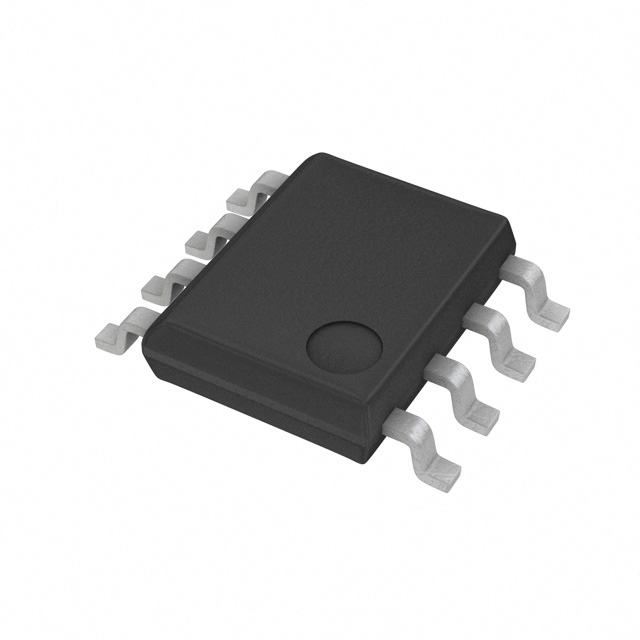
The TSU112IYST is a high-performance, dual-channel CMOS operational amplifier designed for automotive applications. Manufactured by STMicroelectronics, this linear IC chip offers exceptional performance and reliability, making it suitable for a wide range of electronic systems. The TSU112IYST features a wide supply voltage range from 1.5 V to 5.5 V, allowing for flexibility in power supply design. Its low input bias current of 1 pA ensures minimal loading effects on sensitive input sources, while the low input offset voltage of 150 µV guarantees high accuracy in signal processing.
TSU112IYST Features
- Amplifier Type: CMOS
- Number of Circuits: 2
- Voltage - Supply Span (Min/Max): 1.5 V to 5.5 V
- Gain Bandwidth Product: 9 kHz
- Slew Rate: 0.0031 V/µs
- Current - Input Bias: 1 pA
- Current - Supply: 1µA (per channel)
- Current - Output / Channel: 45 mA
- Voltage - Input Offset: 150 µV
- Mounting Type: Surface Mount
- Package: Tape & Reel (TR)
- Moisture Sensitivity Level (MSL): 1 (Unlimited)
- Product Status: Active
- REACH Status: REACH Unaffected
- RoHS Status: ROHS3 Compliant
- Grade: Automotive
TSU112IYST Applications
The TSU112IYST is ideal for applications requiring high precision and low power consumption. Its automotive grade certification ensures robustness and reliability in demanding environments. Specific use cases include:
- Automotive Electronics: Suitable for automotive sensor interfaces, where high accuracy and low power consumption are critical.
- Signal Conditioning: Ideal for conditioning low-level signals in various electronic systems, ensuring minimal distortion and high fidelity.
- Battery-Powered Devices: The low supply current of 1µA per channel makes it perfect for battery-powered applications, extending operational life.
- Precision Measurement Equipment: The low input bias current and offset voltage make it suitable for precision measurement applications, providing accurate and reliable results.
Conclusion of TSU112IYST
The TSU112IYST from STMicroelectronics stands out as a versatile and reliable dual-channel CMOS operational amplifier tailored for automotive applications. Its wide supply voltage range, low power consumption, and high precision make it an excellent choice for a variety of electronic systems. The TSU112IYST's compliance with automotive standards and environmental regulations further enhances its suitability for modern, high-performance applications. Whether used in automotive electronics, signal conditioning, or precision measurement, the TSU112IYST delivers outstanding performance and reliability, making it a preferred choice for engineers and designers in the electronics industry.
Tech Specifications
TSU112IYST Documents
Download datasheets and manufacturer documentation for TSU112IYST
 TSU111IY, TSU112IY
 Shopping Guide


.png?x-oss-process=image/format,webp/resize,h_32)


