
 German
 Japanese
 Portuguese
 Korea
Korea
 Mexico
 Dutch
Dutch


STMicroelectronics
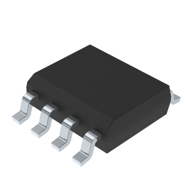
TSV358AIYDT
Why Choose Us?
Professional Platform
B2B & B2C purchasingDelivery at full speed
1-2 days deliveryWide variety
Original manufacturers365 days guarantee
Responsible quality
.png)


Tech Specifications
TSV358AIYDT Description
TSV358AIYDT Description
The TSV358AIYDT is a high-performance operational amplifier (op-amp) from STMicroelectronics, designed for a wide range of applications in the automotive industry. This dual-channel op-amp offers excellent technical specifications, making it ideal for various applications where high precision and reliability are required.
TSV358AIYDT Features
- Voltage - Supply Span (Min): 2.5 V - Voltage - Supply Span (Max): 6 V: The TSV358AIYDT can operate over a wide voltage range, providing flexibility in various power supply scenarios.
- Gain Bandwidth Product: 1.4 MHz: This high gain bandwidth product ensures fast response times and excellent performance in high-frequency applications.
- Slew Rate: 0.6V/µs: The TSV358AIYDT's high slew rate allows for quick signal transitions, making it suitable for applications requiring fast response times.
- Current - Input Bias: 70 nA - Current - Supply: 500µA: The low input bias and supply currents contribute to the op-amp's low power consumption, making it ideal for battery-powered applications.
- Voltage - Input Offset: 100 µV: The low input offset voltage ensures high accuracy and precision in signal processing.
- Current - Output / Channel: 80 mA: The TSV358AIYDT can provide ample current to drive various loads, making it suitable for a wide range of applications.
- Mounting Type: Surface Mount: The surface-mount packaging allows for easy integration into modern electronic devices.
- Number of Circuits: 2: The dual-channel design enables the use of a single op-amp for two separate signal processing tasks, reducing component count and board space.
- Grade: Automotive: The TSV358AIYDT is designed to meet the stringent requirements of automotive applications, ensuring reliability and performance in harsh environments.
- REACH Status: REACH Unaffected - RoHS Status: ROHS3 Compliant: The TSV358AIYDT complies with environmental regulations, making it suitable for environmentally conscious designs.
- Moisture Sensitivity Level (MSL): 1 (Unlimited): The op-amp has a high moisture sensitivity level, allowing for extended storage and handling without compromising performance.
TSV358AIYDT Applications
The TSV358AIYDT is ideal for a wide range of applications in the automotive industry, including:
- Sensor Signal Conditioning: The high precision and low noise characteristics make it suitable for conditioning signals from various sensors in automotive systems.
- Audio Amplification: The dual-channel design and high slew rate make it ideal for audio amplification applications, such as car audio systems.
- Data Acquisition Systems: The TSV358AIYDT can be used in data acquisition systems for processing and amplifying signals from various sensors in automotive applications.
- Control Systems: The high gain bandwidth product and low input bias current make it suitable for control systems in automotive applications, such as engine control units (ECUs) and transmission control units (TCUs).
Conclusion of TSV358AIYDT
The TSV358AIYDT is a versatile and high-performance operational amplifier from STMicroelectronics, designed for a wide range of automotive applications. Its excellent technical specifications, low power consumption, and compliance with environmental regulations make it an ideal choice for demanding applications where reliability and performance are critical. With its dual-channel design, the TSV358AIYDT offers a cost-effective and space-saving solution for various signal processing tasks in the automotive industry.
FAQ
Not available to buy online? Want the lower wholesale price? Please Send RFQ to get best price, we will respond immediately


.png?x-oss-process=image/format,webp/resize,h_32)


