

STMicroelectronics
TSV358IYDT
OP Amps, Buffer Amps ICs
Not available to buy online? Want the lower wholesale price? Please Send RFQ to get best price, we will respond immediately


.png?x-oss-process=image/format,webp/resize,p_30)


TSV358IYDT Description
TSV358IYDT Description
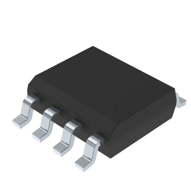
The TSV358IYDT is a high-performance operational amplifier (op-amp) from STMicroelectronics, designed for a wide range of applications in the electronics industry. This op-amp is part of the TSV358 series and is specifically designed for general-purpose applications. It is available in an 8-SOIC package and is RoHS3 compliant, making it suitable for use in various electronic devices.
TSV358IYDT Features
- Voltage Supply Span: The TSV358IYDT operates over a wide voltage range of 2.5 V to 6 V, providing flexibility in power supply design.
- Gain Bandwidth Product: With a gain bandwidth product of 1.4 MHz, the TSV358IYDT offers excellent high-frequency performance.
- Slew Rate: The op-amp has a slew rate of 0.6 V/µs, ensuring fast response times in high-speed applications.
- Input Bias Current: The low input bias current of 70 nA contributes to the op-amp's high input impedance and low power consumption.
- Supply Current: The TSV358IYDT consumes only 500 µA of supply current, making it energy-efficient.
- Input Offset Voltage: The low input offset voltage of 200 µV ensures high accuracy in signal processing.
- Output Current: Each channel can deliver up to 80 mA of output current, providing sufficient drive capability for various loads.
- Number of Circuits: The TSV358IYDT features two independent op-amp circuits in a single package, offering cost and space savings.
- Mounting Type: The surface-mount packaging allows for easy integration into printed circuit boards (PCBs).
TSV358IYDT Applications
The TSV358IYDT is an ideal choice for various applications due to its excellent performance and versatility:
- Audio Amplification: The low noise and high slew rate make it suitable for audio applications, such as preamplifiers and audio mixers.
- Sensor Signal Conditioning: The low input offset voltage and low bias current make it ideal for conditioning signals from sensors in industrial and automotive applications.
- Data Acquisition Systems: The high gain bandwidth product and low input bias current make the TSV358IYDT suitable for use in data acquisition systems, where accurate signal processing is critical.
- Automotive Applications: The automotive-grade rating and wide supply voltage range make it suitable for use in various automotive electronic systems, such as engine control units and infotainment systems.
Conclusion of TSV358IYDT
The TSV358IYDT is a versatile and high-performance operational amplifier from STMicroelectronics, offering excellent technical specifications and performance benefits. Its wide voltage supply range, low power consumption, and high slew rate make it suitable for a wide range of applications, including audio amplification, sensor signal conditioning, data acquisition systems, and automotive electronics. With its unique features and advantages over similar models, the TSV358IYDT is an excellent choice for designers looking for a reliable and cost-effective op-amp solution.
Tech Specifications
TSV358IYDT Documents
Download datasheets and manufacturer documentation for TSV358IYDT
 TSV321(A), 358(A), 324(A) TSV358 View All Specifications TSV321(A), 358(A), 324(A)
 Related Parts


Shopping Guide


.png?x-oss-process=image/format,webp/resize,h_32)


©2025 ERSA Electronics Corporation.