
STMicroelectronics
TSV622IST
OP Amps, Buffer Amps ICs

Not available to buy online? Want the lower wholesale price? Please Send RFQ to get best price, we will respond immediately


.png?x-oss-process=image/format,webp/resize,p_30)


TSV622IST Description
TSV622IST Description
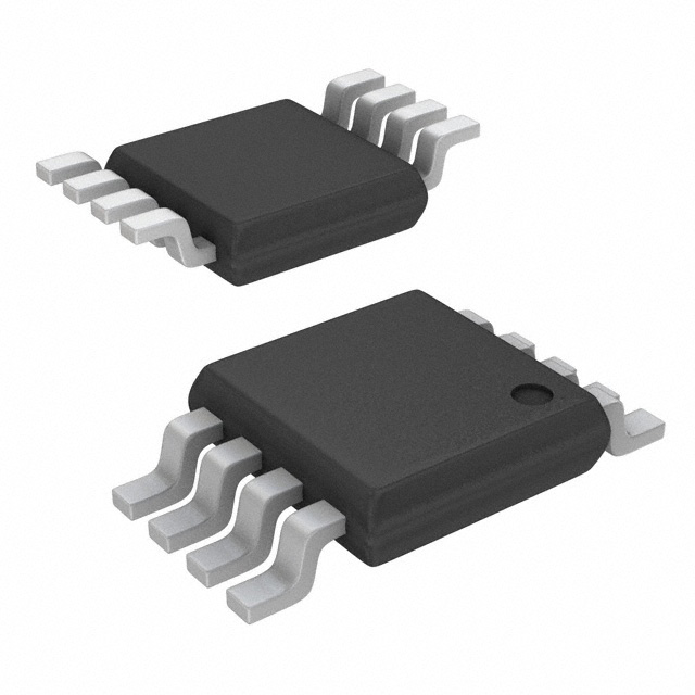
The TSV622IST is a high-performance, dual CMOS operational amplifier offered by STMicroelectronics. This device is designed to provide exceptional performance in a wide range of applications, thanks to its versatile operating voltage range, low input bias current, and high slew rate. The TSV622IST features a supply voltage span ranging from 1.5 V to 5.5 V, making it suitable for both low-power and standard voltage applications. Its gain bandwidth product of 420 kHz ensures stable and precise signal processing, while the low input bias current of 1 pA minimizes signal distortion. The amplifier's supply current of 29µA and output current per channel of 74 mA further enhance its efficiency and robustness. The TSV622IST is packaged in a surface-mount, 8-pin mini-SO package, which is ideal for compact designs and high-density PCB layouts.
TSV622IST Features
- Wide Operating Voltage Range: The TSV622IST operates from 1.5 V to 5.5 V, providing flexibility for various power supply configurations.
- Low Input Bias Current: With an input bias current of just 1 pA, the TSV622IST minimizes the impact on sensitive input signals, ensuring high accuracy and reliability.
- High Gain Bandwidth Product: The 420 kHz gain bandwidth product enables the amplifier to handle a wide range of frequencies with minimal phase shift and distortion.
- High Slew Rate: The 0.14 V/µs slew rate ensures fast response times, making the TSV622IST suitable for applications requiring quick signal transitions.
- Low Supply Current: The 29µA supply current per amplifier allows for low power consumption, which is crucial for battery-powered and energy-efficient designs.
- High Output Current: The ability to deliver up to 74 mA per channel makes the TSV622IST robust and capable of driving heavy loads.
- Surface-Mount Package: The 8-pin mini-SO package is ideal for compact and high-density PCB layouts, facilitating easy integration into modern electronic designs.
- Compliance and Reliability: The TSV622IST is REACH unaffected and RoHS3 compliant, ensuring environmental sustainability and regulatory adherence. It also has a moisture sensitivity level (MSL) of 1, making it suitable for unlimited storage conditions.
TSV622IST Applications
The TSV622IST is well-suited for a variety of applications due to its versatile performance characteristics. Some key applications include:
- Signal Conditioning: Ideal for amplifying and conditioning weak signals in sensor interfaces, ensuring accurate and reliable data transmission.
- Analog-to-Digital Conversion: The low input bias current and high gain bandwidth product make it suitable for driving ADCs, providing high-fidelity signal conversion.
- Audio Amplification: The TSV622IST can be used in audio circuits to amplify and process audio signals, delivering clear and distortion-free sound.
- Power Management: Its low supply current and wide operating voltage range make it suitable for power management applications, where efficiency and flexibility are critical.
- Industrial Control Systems: The robustness and high output current capability of the TSV622IST make it ideal for industrial control systems, where reliable signal processing and load driving are essential.
Conclusion of TSV622IST
The TSV622IST from STMicroelectronics is a versatile and high-performance dual CMOS operational amplifier that offers a wide range of benefits for various electronic applications. Its wide operating voltage range, low input bias current, high gain bandwidth product, and high slew rate make it an excellent choice for signal conditioning, audio amplification, and power management. The low supply current and high output current further enhance its efficiency and robustness, making it suitable for both low-power and high-load applications. The surface-mount package and compliance with environmental regulations ensure easy integration and sustainability. Overall, the TSV622IST stands out as a reliable and efficient solution for modern electronic designs.
Tech Specifications
TSV622IST Documents
Download datasheets and manufacturer documentation for TSV622IST
TSV62x(A) TSV622 View All Specifications TSV62x(A) Related Parts


Shopping Guide


.png?x-oss-process=image/format,webp/resize,h_32)


©2025 ERSA Electronics Corporation.