
 German
 Japanese
 Portuguese
 Korea
Korea
 Mexico
 Dutch
Dutch


STMicroelectronics
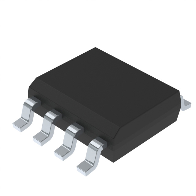
TSV7722IYDT

Why Choose Us?
Professional Platform
B2B & B2C purchasingDelivery at full speed
1-2 days deliveryWide variety
Original manufacturers365 days guarantee
Responsible quality
.png)


Tech Specifications
TSV7722IYDT Description
TSV7722IYDT Description
The TSV7722IYDT is a high-performance, dual-channel general-purpose operational amplifier (op-amp) designed by STMicroelectronics. This device is optimized for a wide range of applications requiring high slew rate, low input bias current, and low input offset voltage. The TSV7722IYDT features a gain bandwidth product of 22 MHz and a slew rate of 11V/µs, making it suitable for high-speed signal processing and amplification tasks. The op-amp is designed for surface mount technology, ensuring ease of integration into modern electronic circuits.
TSV7722IYDT Features
- High Slew Rate: The TSV7722IYDT boasts a high slew rate of 11V/µs, which is crucial for applications requiring fast signal transitions and minimal distortion.
- Low Input Bias Current: With an input bias current of only 2 pA, the TSV7722IYDT minimizes the impact of input currents on the signal, ensuring high accuracy and stability in precision applications.
- Low Input Offset Voltage: The device features a low input offset voltage of 50 µV, which is essential for maintaining signal integrity and reducing errors in sensitive circuits.
- Dual Channel Design: The TSV7722IYDT includes two independent op-amp channels, each capable of delivering 70 mA of output current, providing flexibility and efficiency in multi-channel applications.
- Low Power Consumption: The op-amp operates with a supply current of 1.7mA per channel, making it suitable for low-power and battery-operated devices.
- Surface Mount Packaging: The TSV7722IYDT is available in a surface mount package, facilitating easy integration into compact and high-density PCB designs.
- Compliance and Reliability: The device is REACH unaffected and RoHS3 compliant, ensuring environmental sustainability and reliability in various industrial applications. The moisture sensitivity level (MSL) of 1 (unlimited) further enhances its robustness and suitability for diverse operating conditions.
TSV7722IYDT Applications
The TSV7722IYDT is ideal for a variety of applications that demand high performance and reliability. Some specific use cases include:
- Analog Signal Processing: The high slew rate and gain bandwidth product make it suitable for applications involving high-speed analog signal processing, such as in audio and video equipment.
- Precision Measurement: The low input bias current and low input offset voltage ensure high accuracy in precision measurement instruments, such as in medical devices and industrial sensors.
- Power Management: The dual-channel design and high output current capability make it ideal for power management applications, including voltage regulators and motor control systems.
- Consumer Electronics: The TSV7722IYDT can be used in consumer electronics for signal amplification and processing, ensuring high performance and reliability in devices such as smartphones, tablets, and home appliances.
Conclusion of TSV7722IYDT
The TSV7722IYDT from STMicroelectronics is a versatile and high-performance dual-channel op-amp that offers significant advantages over similar models. Its high slew rate, low input bias current, and low input offset voltage make it ideal for a wide range of applications requiring precision and high-speed signal processing. The device's low power consumption, surface mount packaging, and compliance with environmental standards further enhance its appeal for modern electronic designs. Whether used in consumer electronics, precision instruments, or power management systems, the TSV7722IYDT delivers reliable performance and exceptional value.
FAQ
| Quantity | Unit Price | Ext. Price |
|---|---|---|
| 1+ | $1.28400 | $1.28 |
| 10+ | $1.25315 | $12.53 |
| 30+ | $1.23257 | $36.98 |
Not available to buy online? Want the lower wholesale price? Please Send RFQ to get best price, we will respond immediately


.png?x-oss-process=image/format,webp/resize,h_32)


