
STMicroelectronics
TSV852AIST
OP Amps, Buffer Amps ICs


.png?x-oss-process=image/format,webp/resize,p_30)


TSV852AIST Description
TSV852AIST Description
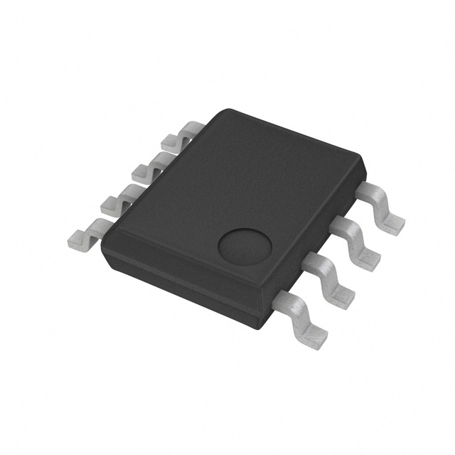
The TSV852AIST is a high-performance, general-purpose operational amplifier designed by STMicroelectronics, a leading manufacturer in the semiconductor industry. This dual-channel op-amp is optimized for automotive applications, ensuring robust performance in demanding environments. The TSV852AIST features a wide supply voltage range, from 2.5 V to 5.5 V, making it suitable for a variety of power supply configurations. It offers a gain bandwidth product of 1.3 MHz and a slew rate of 0.7 V/µs, ensuring high-speed signal processing capabilities. The device also boasts low input bias current of 27 nA and an input offset voltage of 800 µV, contributing to its precision and stability. With a supply current of 130 µA per channel and an output current of 70 mA per channel, the TSV852AIST provides efficient power management and strong drive capabilities. Packaged in a surface-mount 8-MiniSO format, it is ideal for compact designs and easy integration into modern electronic systems. The TSV852AIST is REACH unaffected and RoHS3 compliant, ensuring environmental sustainability and regulatory compliance.
TSV852AIST Features
- Wide Supply Voltage Range: Operates from 2.5 V to 5.5 V, providing flexibility in power supply design.
- High Gain Bandwidth Product: 1.3 MHz ensures high-frequency performance and fast signal processing.
- Low Input Bias Current: 27 nA minimizes offset errors and improves precision in sensitive applications.
- Low Input Offset Voltage: 800 µV ensures accurate signal amplification and reduces errors.
- High Slew Rate: 0.7 V/µs allows for rapid response to input signal changes, ideal for dynamic systems.
- Efficient Power Management: 130 µA supply current per channel ensures low power consumption.
- Strong Output Drive: 70 mA output current per channel provides robust performance.
- Surface-Mount Packaging: 8-MiniSO format is compact and suitable for space-constrained designs.
- Automotive Grade: Designed to meet the stringent requirements of automotive applications.
- Environmental Compliance: REACH unaffected and RoHS3 compliant, ensuring sustainability and regulatory adherence.
TSV852AIST Applications
The TSV852AIST is well-suited for a variety of applications, particularly in the automotive sector. Its robust performance and automotive-grade reliability make it ideal for:
- Automotive Electronics: Use in engine control units, transmission control systems, and advanced driver-assistance systems (ADAS).
- Signal Conditioning: Amplifying and conditioning signals in sensors and transducers.
- Power Management: Managing power in automotive electronic systems, ensuring efficient energy use.
- Industrial Control: Controlling and monitoring industrial processes, ensuring precise and reliable operation.
- Consumer Electronics: Enhancing performance in consumer devices that require high precision and low power consumption.
Conclusion of TSV852AIST
The TSV852AIST from STMicroelectronics is a versatile and high-performance general-purpose operational amplifier tailored for automotive and industrial applications. Its wide supply voltage range, high gain bandwidth product, and low input bias current make it an excellent choice for precision signal processing. The device’s low power consumption and strong output drive capabilities ensure efficient operation and robust performance. With its compact surface-mount packaging and environmental compliance, the TSV852AIST is an ideal solution for modern electronic systems requiring reliability, precision, and sustainability.
Tech Specifications
TSV852AIST Documents
Download datasheets and manufacturer documentation for TSV852AIST
 TSV85x(A)
  TSV852A View All Specifications
  TSV85x(A)
 Shopping Guide


.png?x-oss-process=image/format,webp/resize,h_32)


