
STMicroelectronics
TSV912AIYDT
OP Amps, Buffer Amps ICs


.png?x-oss-process=image/format,webp/resize,p_30)


TSV912AIYDT Description
TSV912AIYDT Description
The TSV912AIYDT is a high-performance operational amplifier (op-amp) designed and manufactured by STMicroelectronics. This device is part of the OP Amps, Buffer Amps ICs category and is specifically tailored for automotive applications. With its robust features and specifications, the TSV912AIYDT offers superior performance and reliability in various electronic systems.
TSV912AIYDT Features
- Voltage Supply Span: The TSV912AIYDT operates within a wide voltage range, from a minimum of 2.5 V to a maximum of 5.5 V, ensuring compatibility with various power sources.
- Gain Bandwidth Product: This op-amp boasts an impressive gain bandwidth product of 8 MHz, enabling high-speed signal processing.
- Slew Rate: The device features a fast slew rate of 4.5V/µs, which is crucial for handling rapidly changing input signals.
- Input Bias Current: With an ultra-low input bias current of 1 pA, the TSV912AIYDT minimizes input offset errors and ensures accurate signal processing.
- Supply Current: The device consumes a low supply current of 780µA for both channels, making it energy-efficient.
- Output Current: Each channel can deliver up to 35 mA, providing ample current for driving various loads.
- Input Offset Voltage: The TSV912AIYDT has a low input offset voltage of 1.5 mV, contributing to high accuracy in signal amplification.
- Mounting Type: The device is surface-mount, making it suitable for compact and space-constrained applications.
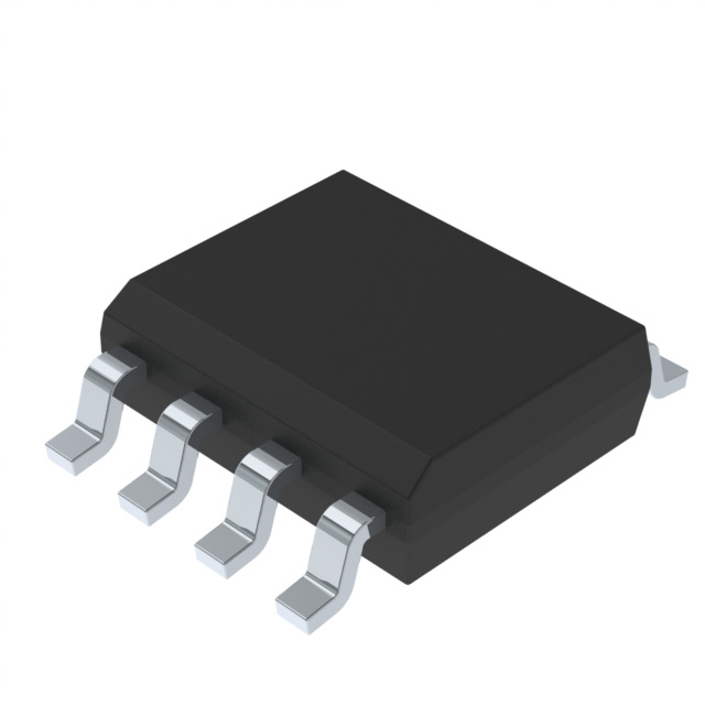
- Package: The TSV912AIYDT is available in an 8-SOIC package, which is both compact and easy to handle.
- Number of Circuits: This op-amp features two independent circuits, doubling the functionality in a single package.
- REACH Status: The TSV912AIYDT is REACH unaffected, ensuring compliance with environmental regulations.
- RoHS Status: The device is RoHS3 compliant, adhering to the European Union's restrictions on hazardous substances.
- Moisture Sensitivity Level (MSL): With an MSL of 1 (Unlimited), the TSV912AIYDT can be stored and handled without concerns about moisture sensitivity.
TSV912AIYDT Applications
The TSV912AIYDT is ideal for a wide range of applications due to its high performance and automotive-grade specifications. Some specific use cases include:
- Automotive Sensor Interfaces: The device's low input bias current and low input offset voltage make it suitable for interfacing with high-precision sensors in automotive systems.
- Audio Amplification: The TSV912AIYDT's high slew rate and gain bandwidth product make it an excellent choice for audio signal amplification in car audio systems.
- Data Acquisition Systems: The device's high-speed performance is well-suited for data acquisition systems in industrial and automotive applications.
- Signal Conditioning: The TSV912AIYDT can be used for signal conditioning in various electronic systems, such as filters, amplifiers, and converters.
Conclusion of TSV912AIYDT
The TSV912AIYDT is a versatile and high-performance operational amplifier designed for automotive applications. Its unique combination of technical specifications, such as a wide voltage supply span, low input bias current, and high slew rate, make it an ideal choice for demanding electronic systems. With its automotive-grade features and compliance with environmental regulations, the TSV912AIYDT is a reliable and efficient solution for a variety of applications in the automotive and industrial sectors.
Tech Specifications
TSV912AIYDT Documents
Download datasheets and manufacturer documentation for TSV912AIYDT
 Product / Process Change Notification (PDF) Product Change Notification (PDF) Product Change Notification 2024-04-18 (PDF)
 Shopping Guide


.png?x-oss-process=image/format,webp/resize,h_32)


