
 German
 Japanese
 Portuguese
 Korea
Korea
 Mexico
 Dutch
Dutch


STMicroelectronics
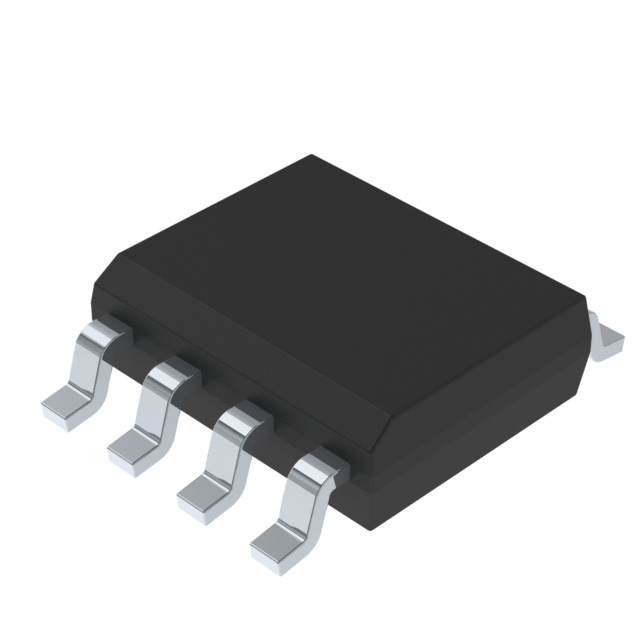
TSX712IYDT

Why Choose Us?
Professional Platform
B2B & B2C purchasingDelivery at full speed
1-2 days deliveryWide variety
Original manufacturers365 days guarantee
Responsible quality
.png)


Tech Specifications
TSX712IYDT Description
TSX712IYDT Description
The TSX712IYDT is a high-performance, automotive-grade operational amplifier (op-amp) from STMicroelectronics. This CMOS-based device is designed for applications requiring low power consumption, high slew rate, and low input bias current. With a supply voltage range of 2.7V to 16V, the TSX712IYDT is suitable for a wide range of electronic systems.
TSX712IYDT Features
- Voltage - Supply Span (Min): 2.7 V
- Voltage - Supply Span (Max): 16 V
- Gain Bandwidth Product: 2.7 MHz
- Slew Rate: 1.4 V/µs
- Current - Input Bias: 1 pA
- Current - Supply: 660 µA (x2 Channels)
- Voltage - Input Offset: 200 µV
- Current - Output / Channel: 50 mA
- Number of Circuits: 2
- Mounting Type: Surface Mount
- Package: Tape & Reel (TR)
- Grade: Automotive
- RoHS Status: ROHS3 Compliant
- REACH Status: REACH Unaffected
- Moisture Sensitivity Level (MSL): 1 (Unlimited)
- ECCN: EAR99
- HTSUS: 8542.33.0001
The TSX712IYDT stands out for its low input bias current, which minimizes errors in precision applications. Its high slew rate ensures fast response times, making it suitable for high-speed signal processing. The automotive-grade rating and compliance with RoHS3 and REACH regulations make it ideal for use in automotive and other regulated industries.
TSX712IYDT Applications
The TSX712IYDT is ideal for a variety of applications, including:
- Automotive Systems: Due to its automotive-grade rating, it is suitable for use in automotive infotainment systems, sensor interfaces, and control systems.
- Industrial Control Systems: Its high slew rate and low input bias current make it suitable for use in precision control systems and signal conditioning applications.
- Medical Equipment: The low input bias current and low noise characteristics make it suitable for use in medical equipment, such as patient monitoring systems and diagnostic devices.
- Consumer Electronics: Its low power consumption and high performance make it suitable for use in portable consumer electronics, such as smartphones, tablets, and wearable devices.
Conclusion of TSX712IYDT
The TSX712IYDT is a versatile, high-performance op-amp that offers a combination of low power consumption, high slew rate, and low input bias current. Its automotive-grade rating and compliance with RoHS3 and REACH regulations make it suitable for use in a wide range of applications, including automotive systems, industrial control systems, medical equipment, and consumer electronics. With its unique features and advantages, the TSX712IYDT is an excellent choice for designers looking for a high-performance op-amp that meets the stringent requirements of regulated industries.
FAQ
Not available to buy online? Want the lower wholesale price? Please Send RFQ to get best price, we will respond immediately


.png?x-oss-process=image/format,webp/resize,h_32)


