
 German
 Japanese
 Portuguese
 Korea
Korea
 Mexico
 Dutch
Dutch


STMicroelectronics
TSX922IYST

Why Choose Us?
Professional Platform
B2B & B2C purchasingDelivery at full speed
1-2 days deliveryWide variety
Original manufacturers365 days guarantee
Responsible quality
.png)


Tech Specifications
TSX922IYST Description
TSX922IYST Description
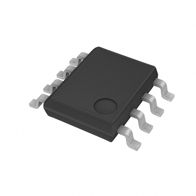
The TSX922IYST is a high-performance CMOS operational amplifier designed by STMicroelectronics, featuring a dual-channel configuration in an 8-pin mini-SOIC package. This automotive-grade IC is optimized for surface-mount applications and offers a wide supply voltage range from 4 V to 16 V, making it suitable for a variety of power supply configurations. The TSX922IYST boasts a gain bandwidth product of 10 MHz and a fast slew rate of 17 V/µs, ensuring high-frequency performance and rapid signal processing. With a low input bias current of 10 pA and an input offset voltage of 5 mV, the amplifier maintains high accuracy and stability. Each channel can deliver an output current of 74 mA, while the total supply current for both channels is 2.8 mA, providing efficient power usage. The TSX922IYST is REACH unaffected and RoHS3 compliant, ensuring environmental and regulatory standards are met. The moisture sensitivity level (MSL) of 1 (unlimited) makes it suitable for various manufacturing environments. Packaged in tape and reel (TR), the TSX922IYST is ready for automated assembly processes.
TSX922IYST Features
- Dual-Channel CMOS Amplifier: The TSX922IYST features two independent CMOS operational amplifier channels, providing flexibility for various signal processing tasks.
- Wide Supply Voltage Range: With a supply voltage range from 4 V to 16 V, the TSX922IYST is versatile and can operate in a wide range of power supply conditions.
- High Gain Bandwidth Product: The 10 MHz gain bandwidth product ensures high-frequency performance, making it suitable for applications requiring fast signal processing.
- Fast Slew Rate: The 17 V/µs slew rate allows for rapid response to input signal changes, minimizing distortion in high-frequency applications.
- Low Input Bias Current: The 10 pA input bias current ensures high input impedance, reducing the loading effect on the signal source and maintaining signal integrity.
- Low Input Offset Voltage: The 5 mV input offset voltage ensures accurate signal amplification, minimizing errors in precision applications.
- High Output Current: Each channel can deliver up to 74 mA, providing robust output drive capability for various loads.
- Efficient Power Usage: The total supply current of 2.8 mA for both channels ensures efficient power consumption, making it suitable for power-sensitive applications.
- Automotive Grade: The TSX922IYST is designed to meet the stringent requirements of automotive applications, ensuring reliability and performance in harsh environments.
- Environmental Compliance: The TSX922IYST is REACH unaffected and RoHS3 compliant, ensuring it meets environmental and regulatory standards.
- Moisture Sensitivity Level 1: The MSL 1 (unlimited) rating makes the TSX922IYST suitable for various manufacturing environments without the need for special handling.
- Tape & Reel Packaging: The TSX922IYST is available in tape and reel (TR) packaging, facilitating automated assembly processes.
TSX922IYST Applications
The TSX922IYST is ideal for a variety of applications due to its high performance and versatility. Some specific use cases include:
- Automotive Electronics: The automotive-grade design makes it suitable for applications such as engine control units, infotainment systems, and advanced driver-assistance systems (ADAS).
- Signal Processing: The high gain bandwidth product and fast slew rate make it ideal for applications requiring high-frequency signal processing, such as audio amplifiers and communication systems.
- Precision Measurement: The low input bias current and low input offset voltage ensure accurate signal amplification, making it suitable for precision measurement applications such as sensors and transducers.
- Power Management: The efficient power usage and high output current capability make it suitable for power management applications, such as voltage regulators and power amplifiers.
- Consumer Electronics: The wide supply voltage range and surface-mount package make it suitable for consumer electronics applications, such as smartphones, tablets, and portable devices.
Conclusion of TSX922IYST
The TSX922IYST is high a-performance CMOS operational amplifier designed for demanding applications in the automotive and electronics industries. Its wide supply voltage range, high gain bandwidth product, and fast slew rate make it suitable for high-frequency signal processing and precision measurement tasks. The low input bias current and low input offset voltage ensure accurate signal amplification, while the high output current capability and efficient power usage make it suitable for a variety of power-sensitive applications. The automotive-grade design and environmental compliance ensure reliability and regulatory compliance. With its versatile features and robust performance, the TSX922IYST is an excellent choice for engineers looking for a reliable and high-performance operational amplifier.
FAQ
Not available to buy online? Want the lower wholesale price? Please Send RFQ to get best price, we will respond immediately


.png?x-oss-process=image/format,webp/resize,h_32)


