
 German
 Japanese
 Portuguese
 Korea
Korea
 Mexico
 Dutch
Dutch


Texas Instruments
74LVC2GU04DCKRG4

Why Choose Us?
Professional Platform
B2B & B2C purchasingDelivery at full speed
1-2 days deliveryWide variety
Original manufacturers365 days guarantee
Responsible quality
.png)


Tech Specifications
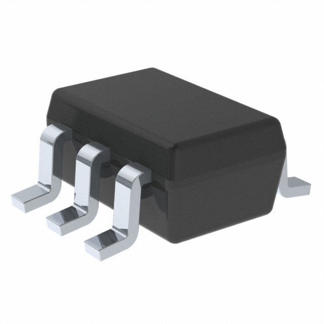
74LVC2GU04DCKRG4 Description
74LVC2GU04DCKRG4 Description
The 74LVC2GU04DCKRG4 is a high-performance, dual-channel inverter IC designed for a wide range of digital logic applications. Manufactured by Texas Instruments, this device is part of the 74LVC series, known for its robustness and versatility. The 74LVC2GU04DCKRG4 features a maximum propagation delay of 3.5ns at 5V and 50pF, ensuring rapid signal processing and minimal latency. It operates within a supply voltage range of 1.65V to 5.5V, making it suitable for various power supply configurations. The device is designed for surface mount applications, packaged in a Tape & Reel (TR) format, and is REACH unaffected and ROHS3 compliant, adhering to stringent environmental and safety standards.
74LVC2GU04DCKRG4 Features
- Logic Type: Inverter
- Number of Circuits: 2
- Number of Inputs: 2
- Input Logic Levels:
- Low: 0.41V to 1.38V
- High: 1.24V to 4.13V
- Propagation Delay: 3.5ns @ 5V, 50pF
- Supply Voltage Range: 1.65V to 5.5V
- Output Current:
- High: 32mA
- Low: 32mA
- Quiescent Current: 10 µA (Max)
- Moisture Sensitivity Level: 1 (Unlimited)
- Mounting Type: Surface Mount
- Package Type: Tape & Reel (TR)
- Compliance: REACH Unaffected, ROHS3 Compliant
74LVC2GU04DCKRG4 Applications
The 74LVC2GU04DCKRG4 is ideal for applications requiring fast and reliable signal inversion. Its low propagation delay and high output current make it suitable for high-speed digital circuits, such as clock signal inversion, data line inversion, and control signal processing. The wide supply voltage range and surface mount packaging ensure compatibility with modern PCB designs and various power supply systems. Specific use cases include:
- Digital Signal Processing: Inverting clock signals in microcontroller and FPGA applications.
- Data Line Management: Inverting data lines in communication interfaces and memory systems.
- Control Signal Inversion: Inverting control signals in digital systems to manage power and enable/disable functions.
- Consumer Electronics: Inverting signals in devices such as smartphones, tablets, and IoT devices.
Conclusion of 74LVC2GU04DCKRG4
The 74LVC2GU04DCKRG4 is a versatile and high-performance inverter IC that offers significant advantages over similar models. Its low propagation delay and high output current ensure rapid and reliable signal inversion, making it ideal for high-speed digital applications. The wide supply voltage range and surface mount packaging provide flexibility in design and compatibility with modern PCB layouts. Compliance with REACH and ROHS3 standards ensures that the device meets stringent environmental and safety requirements. Overall, the 74LVC2GU04DCKRG4 is a reliable choice for engineers and designers seeking a robust inverter solution for their digital logic applications.
FAQ
Not available to buy online? Want the lower wholesale price? Please Send RFQ to get best price, we will respond immediately


.png?x-oss-process=image/format,webp/resize,h_32)


