

Texas Instruments
ADC12C105CISQ
Analog to Digital Converters

Not available to buy online? Want the lower wholesale price? Please Send RFQ to get best price, we will respond immediately


.png?x-oss-process=image/format,webp/resize,p_30)


ADC12C105CISQ Description
ADC12C105CISQ Description
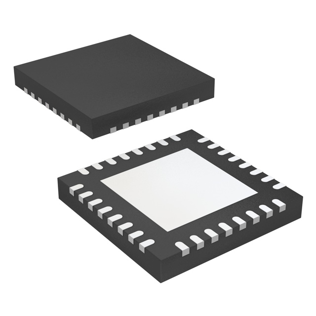
The ADC12C105CISQ is a high-performance 12-bit analog-to-digital converter (ADC) designed by Texas Instruments. This device is part of the ADC12C family and is known for its pipelined architecture, which enables high-speed sampling at a rate of 105 million samples per second (MSPS). The ADC12C105CISQ is housed in a 32-lead WQFN package, making it suitable for surface-mount applications. It features a parallel data interface, allowing for efficient data transfer and integration into various electronic systems.
The ADC12C105CISQ operates with a supply voltage range of 2.7V to 3.6V for both analog and digital supplies, ensuring compatibility with a wide range of power sources. It supports differential input types, which enhance signal integrity and noise rejection, making it ideal for applications where high accuracy and reliability are required. The device also includes both internal and external reference options, providing flexibility in design and calibration.
ADC12C105CISQ Features
- High-Speed Sampling: With a sampling rate of 105 MSPS, the ADC12C105CISQ delivers rapid data acquisition, making it suitable for high-frequency signal processing applications.
- 12-Bit Resolution: The 12-bit resolution ensures precise conversion of analog signals to digital data, providing detailed and accurate measurements.
- Pipelined Architecture: The pipelined architecture allows for continuous data processing, reducing latency and improving overall system performance.
- Differential Inputs: Differential input types minimize noise and interference, ensuring high signal integrity and accuracy.
- Flexible Power Supply: The ADC12C105CISQ operates within a wide voltage range (2.7V to 3.6V) for both analog and digital supplies, offering compatibility with various power sources.
- Parallel Data Interface: The parallel interface facilitates fast and efficient data transfer, enhancing system performance.
- Internal and External Reference Options: The availability of both internal and external reference types provides flexibility in design and calibration, catering to different application requirements.
- Moisture Sensitivity Level (MSL) 3: The MSL 3 rating ensures the device can withstand up to 168 hours of exposure to moisture, making it suitable for a variety of environmental conditions.
ADC12C105CISQ Applications
The ADC12C105CISQ is well-suited for a range of applications where high-speed, high-resolution analog-to-digital conversion is required. Some specific use cases include:
- Communication Systems: High-speed data acquisition in communication systems, such as base stations and transceivers, where rapid signal processing is essential.
- Medical Imaging: Applications in medical imaging equipment, such as ultrasound and MRI machines, where precise and fast signal conversion is critical for accurate diagnostics.
- Industrial Automation: Use in industrial control systems for real-time monitoring and control of processes, ensuring high accuracy and reliability.
- Aerospace and Defense: High-performance signal processing in aerospace and defense applications, where robustness and precision are paramount.
Conclusion of ADC12C105CISQ
The ADC12C105CISQ from Texas Instruments is a robust and high-performance 12-bit ADC designed for demanding applications requiring rapid and accurate signal conversion. Its pipelined architecture, differential inputs, and wide supply voltage range make it a versatile and reliable choice for various industries. Despite its obsolete status, the ADC12C105CISQ remains a valuable component for applications where its unique features and performance benefits are essential.
Tech Specifications
ADC12C105CISQ Documents
Download datasheets and manufacturer documentation for ADC12C105CISQ
ADC12C105 ADC12C105 Related Parts


Shopping Guide


.png?x-oss-process=image/format,webp/resize,h_32)


©2025 ERSA Electronics Corporation.