
 German
 Japanese
 Portuguese
 Korea
Korea
 Mexico
 Dutch
Dutch


Texas Instruments
ADC12DL040CIVS

Why Choose Us?
Professional Platform
B2B & B2C purchasingDelivery at full speed
1-2 days deliveryWide variety
Original manufacturers365 days guarantee
Responsible quality
.png)


Tech Specifications
ADC12DL040CIVS Description
ADC12DL040CIVS Description
The ADC12DL040CIVS is a high-performance analog-to-digital converter (ADC) designed by Texas Instruments. It features a pipelined architecture with 12-bit resolution and a sampling rate of 40 million samples per second (MSPS). This ADC is equipped with two analog-to-digital converters, each with a single-ended input, making it suitable for applications requiring simultaneous sampling of two signals. The device operates with a supply voltage range of 2.7V to 3.6V for the analog section and 2.4V to 3.6V for the digital section, ensuring compatibility with a wide range of power supplies.
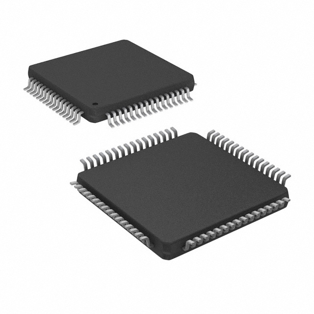
The ADC12DL040CIVS is housed in a 64-pin TQFP package, which is ideal for surface-mount applications. It features a parallel data interface, allowing for efficient data transfer and integration with various digital systems. The device includes both internal and external reference options, providing flexibility in calibration and accuracy requirements. Additionally, it supports differential input types, enhancing signal integrity and noise rejection.
ADC12DL040CIVS Features
- High Sampling Rate: The ADC12DL040CIVS offers a sampling rate of 40 MSPS, making it suitable for high-speed signal processing applications.
- 12-Bit Resolution: Provides precise analog-to-digital conversion with a high level of accuracy.
- Simultaneous Sampling: Two ADCs allow for the simultaneous sampling of two signals, which is crucial for applications requiring synchronized data acquisition.
- Flexible Power Supply: Operates within a voltage range of 2.7V to 3.6V for the analog supply and 2.4V to 3.6V for the digital supply, ensuring compatibility with various power sources.
- Parallel Data Interface: Facilitates efficient data transfer and integration with digital systems.
- Differential Inputs: Enhances signal integrity and noise rejection, making it suitable for high-precision applications.
- Internal and External Reference: Provides flexibility in calibration and accuracy requirements.
- Pipelined Architecture: Ensures high throughput and low latency, making it ideal for real-time signal processing.
ADC12DL040CIVS Applications
The ADC12DL040CIVS is well-suited for a variety of applications that demand high-speed, high-precision analog-to-digital conversion. Some specific use cases include:
- Medical Imaging: Ideal for applications such as ultrasound and MRI systems, where simultaneous sampling and high-speed data acquisition are critical.
- Radar Systems: Suitable for radar signal processing, where the device's high sampling rate and precision are essential for accurate detection and tracking.
- Communication Systems: Useful in high-speed communication systems, where the ADC's ability to handle differential inputs and provide precise data conversion is beneficial.
- Industrial Automation: Applicable in industrial control systems that require real-time signal processing and high-precision data acquisition.
Conclusion of ADC12DL040CIVS
The ADC12DL040CIVS from Texas Instruments is a versatile and high-performance ADC designed for demanding applications. Its 12-bit resolution, 40 MSPS sampling rate, and simultaneous sampling capabilities make it an excellent choice for applications requiring precise and synchronized data acquisition. The device's flexible power supply options, differential inputs, and pipelined architecture further enhance its performance and reliability. While the product is now obsolete, its technical specifications and performance benefits continue to make it a valuable reference for engineers and designers in the electronics industry.
FAQ
Not available to buy online? Want the lower wholesale price? Please Send RFQ to get best price, we will respond immediately


.png?x-oss-process=image/format,webp/resize,h_32)


