
Texas Instruments
ADC12QJ1600AAVTQ1
Analog to Digital Converters


.png?x-oss-process=image/format,webp/resize,p_30)


ADC12QJ1600AAVTQ1 Description
ADC12QJ1600AAVTQ1 Description
The ADC12QJ1600AAVTQ1 is a high-performance Analog-to-Digital Converter (ADC) from Texas Instruments, designed for demanding applications requiring high-speed data acquisition and precision. This 12-bit ADC features a sampling rate of 1.6 Giga-samples per second (GSPS), making it ideal for applications that demand rapid data processing and high accuracy. The ADC12QJ1600AAVTQ1 is equipped with four A/D converters, each capable of handling differential and single-ended inputs, providing flexibility in signal acquisition.
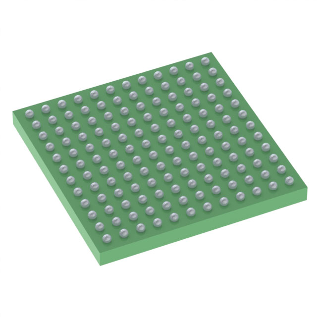
The device supports both JESD204C and SPI data interfaces, ensuring compatibility with a wide range of digital systems. It operates with a supply voltage range of 1.05V to 1.15V for both analog and digital supplies, and an additional 1.8V to 2V supply for analog functions. This ADC is designed for automotive applications, meeting the stringent requirements of the automotive grade, and is available in a surface-mount 144FCBGA package, suitable for compact and reliable designs.
ADC12QJ1600AAVTQ1 Features
- High-Speed Sampling: With a sampling rate of 1.6 GSPS, the ADC12QJ1600AAVTQ1 ensures rapid data acquisition, making it suitable for high-frequency signal processing.
- 12-Bit Resolution: Provides high precision in converting analog signals to digital data, suitable for applications requiring detailed signal analysis.
- Multiple A/D Converters: The four integrated A/D converters allow for simultaneous processing of multiple signals, enhancing the efficiency of data acquisition systems.
- Flexible Data Interfaces: Support for both JESD204C and SPI interfaces ensures compatibility with various digital systems, facilitating seamless integration.
- Wide Supply Voltage Range: Operates within a supply voltage range of 1.05V to 1.15V for analog and digital supplies, and 1.8V to 2V for analog functions, providing flexibility in power management.
- Temperature Sensor: Integrated temperature sensor allows for real-time monitoring of operating conditions, enhancing system reliability.
- Automotive Grade: Designed to meet the stringent requirements of automotive applications, ensuring robustness and reliability in harsh environments.
- RoHS3 Compliant: Adheres to environmental standards, making it suitable for environmentally conscious designs.
- REACH Unaffected: Complies with REACH regulations, ensuring safety and environmental sustainability.
ADC12QJ1600AAVTQ1 Applications
The ADC12QJ1600AAVTQ1 is ideal for a variety of applications, including:
- Automotive Radar Systems: High-speed sampling and precision make it suitable for advanced driver-assistance systems (ADAS) and autonomous driving applications.
- High-Frequency Signal Processing: Ideal for applications requiring rapid data acquisition and processing, such as communication systems and instrumentation.
- Medical Imaging: Provides high-resolution data acquisition for medical imaging devices, enhancing diagnostic capabilities.
- Industrial Automation: Suitable for real-time monitoring and control systems in industrial environments, ensuring precise and reliable operation.
Conclusion of ADC12QJ1600AAVTQ1
The ADC12QJ1600AAVTQ1 from Texas Instruments is a versatile and high-performance ADC designed to meet the demands of modern data acquisition systems. Its high-speed sampling rate, 12-bit resolution, and multiple A/D converters make it an excellent choice for applications requiring rapid and precise data processing. The support for both JESD204C and SPI interfaces, along with its automotive-grade robustness, ensures compatibility and reliability in a wide range of applications. The integrated temperature sensor and compliance with environmental standards further enhance its suitability for modern, high-performance designs.
Tech Specifications
ADC12QJ1600AAVTQ1 Documents
Download datasheets and manufacturer documentation for ADC12QJ1600AAVTQ1
 Wafer Fab Materials 20/May/2021
  ADC12xJ1600-Q1
  ADC12xJ1600-Q1
 Shopping Guide


.png?x-oss-process=image/format,webp/resize,h_32)


