

Texas Instruments
CD4001BE
Gates and Inverters

Not available to buy online? Want the lower wholesale price? Please Send RFQ to get best price, we will respond immediately


- 1+
- $0.47527
- $0.48
- 10+
- $0.37757
- $3.78
- 25+
- $0.33617
- $8.4
- 100+
- $0.28318
- $28.32

.png?x-oss-process=image/format,webp/resize,p_30)


CD4001BE Description
CD4001BE is a quad 2-input NAND gate integrated circuit (IC) manufactured by Texas Instruments. It belongs to the family of digital logic ICs and is widely used in various digital applications due to its versatility and reliability.
Description:
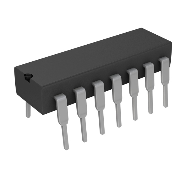
The CD4001BE is a 14-pin DIP (Dual In-line Package) IC, which contains four independent 2-input NAND gates. Each NAND gate is a digital logic gate that performs the inverse of the AND operation. It outputs a low (0) signal only when both of its inputs are high (1). Otherwise, it outputs a high (1) signal.
Features:
- Quad 2-input NAND gate configuration.
- Wide operating voltage range: 2V to 15V.
- High input impedance and low output impedance.
- Compatible with TTL (Transistor-Transistor Logic) and CMOS (Complementary Metal-Oxide-Semiconductor) systems.
- Available in a 14-pin DIP package for easy integration into breadboards or PCBs (Printed Circuit Boards).
- Low power consumption.
- Suitable for both AC and DC applications.
Applications:
- Digital logic circuits: The CD4001BE can be used to design various digital logic circuits, such as decoders, encoders, flip-flops, and counters.
- Boolean algebra simplification: It can be used to simplify Boolean expressions and implement them in hardware.
- Switch debouncing: The NAND gates can be used to debounce mechanical switches, improving the reliability of input signals in digital systems.
- Logic signal inversion: The NAND gate can be used as a simple inverter by connecting one input to a logic high (Vcc) and the other to the input signal.
- Oscillators: The CD4001BE can be used to create simple ring oscillators or other timing circuits.
- Digital signal processing: It can be used in digital signal processing applications, such as filters and waveform generators.
- Educational purposes: The CD4001BE is often used in educational settings to teach the fundamentals of digital logic design and Boolean algebra.
In summary, the CD4001BE is a versatile and reliable quad 2-input NAND gate IC from Texas Instruments, suitable for a wide range of digital applications, including digital logic circuit design, signal processing, and educational purposes. Its compatibility with both TTL and CMOS systems, along with its low power consumption and high input impedance, make it a popular choice for various digital projects.
Tech Specifications
CD4001BE Documents
Download datasheets and manufacturer documentation for CD4001BE
Mechanical Outline Drawing Product Change Notification (PDF) CD4001BE Symbol & Footprint by SnapMagic Logic Guide (Rev. AB) Understanding Buffered and Unbuffered CD4xxxB Series Device Characteristics CD4001B PSPICE Model Related Parts


Shopping Guide


.png?x-oss-process=image/format,webp/resize,h_32)


©2025 ERSA Electronics Corporation.